Unit-19 Electronic Devices
Learning Objectives
After going through this unit, you will be able to understand, appreciate and apply the following concepts:
-
Distinguish between conductors, semi-conductors and insulators.
-
Discuss the intrinsic semi-conductor, its conductivity and factors affecting its conductivity.
-
Appreciate the fact of delibrate addition of impurity in a pure semi-conductor to enhance its conductivity, that is ‘doping process’.
-
Distinguish between p-type and n-type semi-conductor on the basis of nature of dopant (impurity) atom.
-
Discuss the formation of a p-n junction and semi-conductor diode.
-
Discribe the working of a p-n finction diode in forward bias and reverse bias.
-
Discribe the characterstics of an ideal p-n junction diode and sketch its current-voltage relation.
-
Outline the use of several forms of special purpose diodes, including zener diode, LED, photodiode and solar cell.
-
Design a circuit which explains the action of p-n junction diode as rectifier.
-
Explain the basic theory and operation of junction transition (npn configuration as well as pnp configuration).
-
Describe the characterstics of a junction transistor - input characterstics, output characterstics and transfer characterstics.
-
Calculate the input resistance, output resistance and current gains in
-
Describe the switching action of npn transistor in CE configuration by making reference to its voltage (input / output) transfer / mutual characterstics.
-
Describe the amplification or amplifier action of transistor in CE configuration by making reference to output characterstics (a small change in base current leading to comparitvely large change in collector current).
-
Derive the voltage gain, ac current gain and power gain of an amplifier.
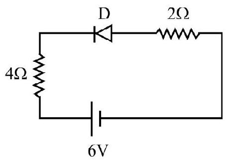
-
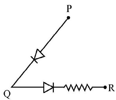
Describe the action of transistor as an oscillator by making reference to feadback process and tank / oscillatoryLC circuit.
-
Distinguish between analogue and digital circuits.
-
Define and describe the basic logic gates OR, AND, NOT, NAND and NOR.
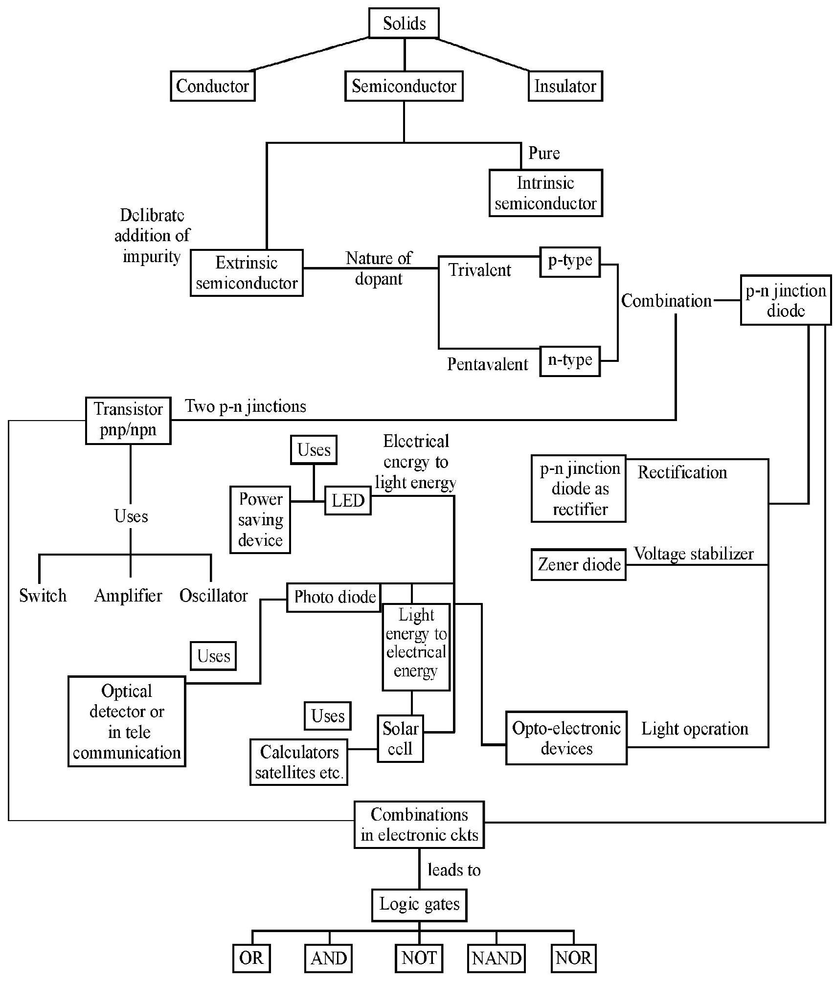
Semiconductor and Electronic Devices
Semiconductors: The semiconductors and solids whose electrical conductivity lies between very high conductivity of metals and very low conductivity of insulators. The pure seminconductors are insulators at very low temperature. Their resistance decreases as their temperature increases, which is a behaviour opposite to that of a metal. The most common semiconductors are elemental semiconductors, example silicon
Classifiction of solids inot conductors, insulators and semiconductors on the basis of energy band diagram

Energy Band
According to Bohr’s theory in an isolated atom; the allowed energy state of an electron depends on the principle quantum number (n).For a particular value of
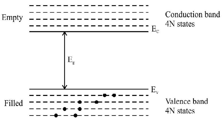
Fig. 1: Energy band positions in a semiconductor at
In a solid we have a large number of atoms/molecules very closely packed. The electron in one atom experience a force due to neighbouring atoms/molecules also. We say we have intracting atoms. To consider the effect of interaction we confine our attention on electrons in the outermost orbit around the atoms (i.e. valency electrons). For “two interacting atoms” we find that for one value of
With no external energy available the valency electrons reside in valence band i.e. energy states in valency band are filled. There are no electrons in conduction band i.e. the conduction band is empty as shown in Fig. 1.
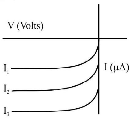
The energy gap Eg may be zero, small or large. This leads to classification of materials as conductors; semiconductor or insulators.
Case-I : Conductors
When the conductioin band is partically filled and valence band is partially empty or when the conduction band and valence band overlap each other
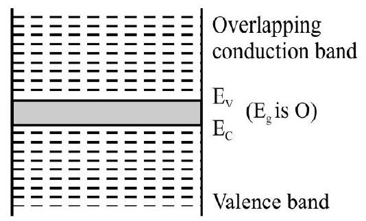
Fig. 2: Mctals or Conductors
Case-II : Insulators
In this case a large energy gap (
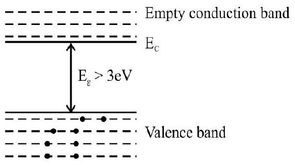
Fig. 3: Insulators
Case-III : Semi-conductors
In this case, there is a finite and a small energy gap
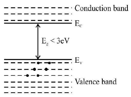
Fig. 4: Semiconductors
Intrinsic Semiconductor
A pure semiconductor, free from any inpurity is called ‘intrinsic’ semiconductor. Its electrical conductivity, which arises by thermal excitation of electrons from the valence band to the conduction band is known as intrinsic conductivity. Most commonly known intrinsic semiconductors are cryslats of Ge and Si. We know that an atom of Si or Ge has four valence electrons. In its crystalline structure, energy Si or Ge atom tends to share one of its four valence electrons with each of its four nearest neighbour atoms and also to take share of one electron from each such neighbour. These shared electron pairs are referred to as forming a covalent bond or valence bond.
At very low temperature, all the valence electrons are tightly bound (all bonds are intact). As the temperature increases, due to thermal excitation, some of there electrons may break-away and cross over to the conduction bond (becomes free electron and available for conduction). This creates a vacancy in the bond. The neighbourhood from which the free electrons
In intrinsic semiconductors, the number of free electrons
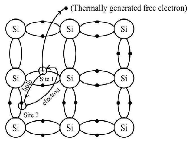
Fig. 4: Schematic model of generation of electron hole pair in silicon crystal
When an electric field is applied to the pure semiconductor, the free elctrons in the conduction band move in a direction opposite to the field, and the holes in the valence band move in the direction of field both giving rise to electric current. (The motion of holes is however, the motion of bounded electrons from one vacancy to the next within the valence band in a direction opposite to the applied field).
Hence, under the action of an electric field, the holes move towards negative potential giving rise to hole current
Fig. (5) shows free electrons in conduction band and holes in valence band in the energy-band diagram.
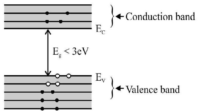
Fig. 5: At
It may be noted that, at equilibrium, the rate of generation of electron-hole pair is equal to the rate of recombination of electron-hole pair.
Extrinic Semiconductor
The conductivity of intrinsic semiconductor depends on its temperature, and very small at room temperature. If, however a small amount of suitable impurity is deliberately added to the pure semiconductor, then the conductivity is significantaly increased. Such materials are known as ’extrinsic’ or ‘doped’ semiconductors. The deliberate addition of a desirable impurity is called doping and the impurity atoms are called dopants.
The dopant has to be such taht it does not distort the original physical and chemical properties of pure crystal.Forthis a small amout say, a few parts per million (impurity atoms per
There are two types of dopants used in doping the letravalent Si or Ge.
(i) Pentavalent - Like Assenic (As), Antimony (Sb), Phosphorous (P) etc.
(ii) Trivalent - Like Indium(In), Boron (B), Aluminium (Al) etc.
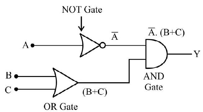
n-type Semiconductor
When a pentavalent impurity (Valency 5) atom is added pure Si or Ge, four of the five valence electrons of the impurity atom form covalent bonds with one each valence electrons of four Ge or Si atoms surrounding
it; while the fifth remains very weakly bound to the parent atom. As a result inonisation energy required to set this electron free is very small and even at room temperature it will be free to move about in the crystal. [For example, the energy required is
In a doped semiconductor the total number of conduction electrons
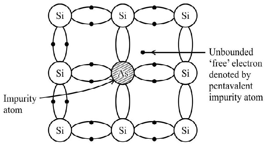
Fig. 6: n-type Semiconductor
p-type Semiconductor
When a trivalent inpurity (valency 3) atom is added to pure
This phenomenon continuous, these holes are in addition to the intrinsically generated hole, while the source of conduction (free) electrons is only intrinsic generation. Thus, for such a material, the holes are the majority carriers and electrons are minority carriers. Therefore, extrinsic semiconductor doped with privalent impurity is called
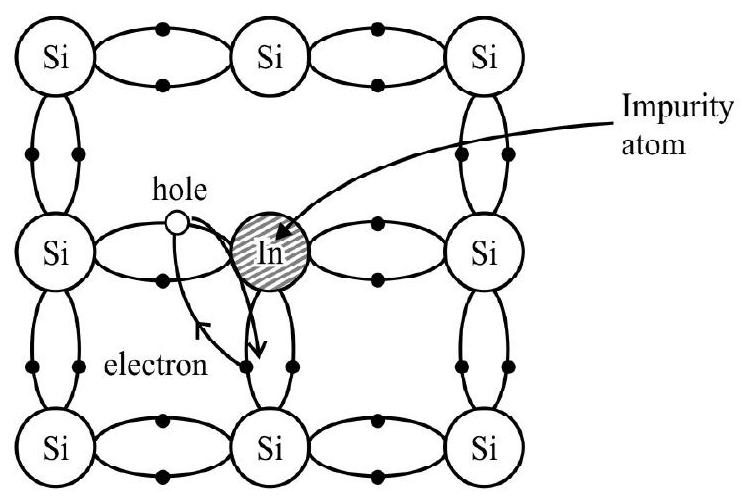
Fig. 7: p-type Semiconductor
Important Conclusion
(i) Extrinsic semiconductor (n-type or p-type) maintains an overall charge neutrality as the charge of additional charge carriers is just equal and opposite to that of ionised cores in the lattice (Crystal).
(ii) The electron hole concentration in an extrinsic semiconductor in thermal equilibrium is given by
(iii) The semiconductors energy band structure is affected by doping. In case of exterinsic semiconductors additional energy states due to donor impurities and acceptor impurities also exist. In the energy band diagram of n-type semiconductor, the donor energy level

(iv) Distinction between intrinsic and Extrinsic Semiconductors
| Intrinsic Semiconductor | Extrinsic Semiconductor | ||
|---|---|---|---|
| 1. | It is a pure, natural semiconductor, such as pure |
It is prepared by adding a small quantity of impurity to a pure semiconductor, such as |
|
| 2. | In it the concentrations of electrons and and holes are equal. | In it the two concentrations are unequal. There is an excess of electrons in |
|
| 3. | Its electrical conductivity is very low. | Its electrical conductivity is significantly high. | |
| 4. | Its conductivity cannot be controlled. | Its conductivity can be controlled by adjusting the quantity of the impurity added. | |
| 5. | Its conductivity increases exponentially with temperature. | Its conductivity also increases with temperature, but not exponentially. |
(v) Distinction between
| n-type Semiconductor | p-type Semiconductor | ||
|---|---|---|---|
| 1. | It is an extrinsic semiconductor obtained by adding a pentavelent impurity to a pure intrinsic semiconductor. | It is also an extrinsic semiconductor obtained by adding a trivalent impurity to a pure intrinsic semiconductor. | |
| 2. | The impurity atoms added provide extra free electrons to the crystal lattice and are called donor atoms. | The impurity atoms added create holes in the crystal lattice and are impurity to a pure intrinsic semiconductor. | |
| 3. | The electrons are majority carriers and the holes minority carriers. | The holes are majority carriers and theelectron are minority carreris. | |
| 4. | The electrons concentration is much more than the hole concentration |
The hole concentration is much more than the electron concentration |
Example-1:
The number of silicon atoms per
Show Answer
Solution:
Given
as
For charge neutrality
From (1) & (2), we get
as
Semiconductor material is n-type.
Example-2:
Why does the electrical conductivity of a pure semiconductor increases on heating?
Show Answer
Solution:
As the temperature increases, more and more of the electrons in the valence band gain energy to cross the energy gap and enter the conduction band. This results in an increase in the number of charge carriers. Hence conductivity increases.
Example-3:
Are the mobilities of electron and hole equal in semiconductor.
Show Answer
Solution:
No, the electron mobility is higher than hole mobility because hole mobility is due to bounded electron movement in valence band.
Electrical Conductivity of a Semiconductor Crystal
We now know that when an external electric field is applied, the free electrons move opposite to the field and the holes in the direction of the field, thus constituting current in same direction.
Let us consider a cylinderical semiconductor of length
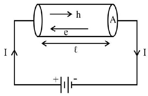
Also total current in the circuit, I will be
or
or
or
With rise in temperature charge carrier concentration increases exponentially whereas mobility (
p-n Junction
A
Formation of
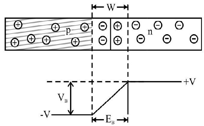
Fig. 9
As soon as junction is formed two important processes occur: diffusion and drift. As we already know that in n-type semiconductors concentration of electrons (free) is more than holes and in p-type concentration of holes is more than electrons. Hence due to the concentration gradient across
This motion of charge carriers give rise to diffusion current across the junction. The diffused chargecarriers combine with their counterparts in the vicinity of the junction and neutralise each other. Thus, in the vicinity of the junction, positive charge (in the form of fixed donor ions) is built on the n-side and negative charge (in the form of fixed accepter ions) on the
The region on either side of the junction which becomes depleted of the mobile charge carriers in called the ‘deplation layer’ or depletion ‘region’. The width of deplation layer is of the order of
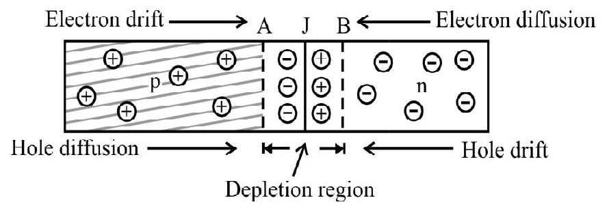
Fig. 10
Semiconductor Diode
A semiconductor diode is basically a
The equilibrium barrier potential ’
(i) By applying external field in the direction opposite to the barrier field (Forward bias).
(ii) By applying external fied in the direction of the barrier field (Reverse bias).
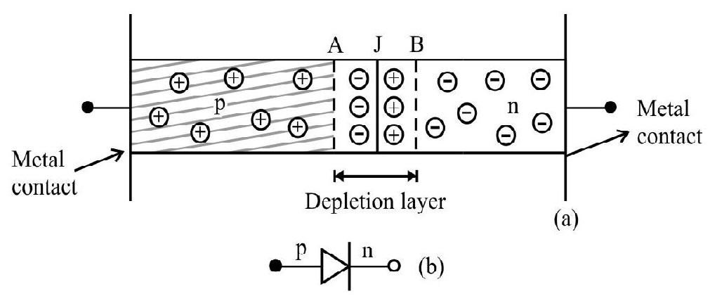
Fig. 11 (a): pn jinction diode (b) symbol
p-n Junction under Forward Bias
When an external voltage is applied across the diode opposite the inbuilt barrier potential
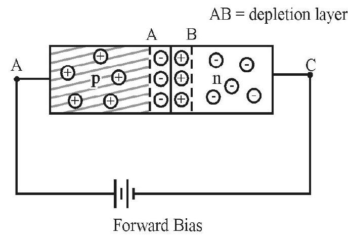
Fig. 12 (a)
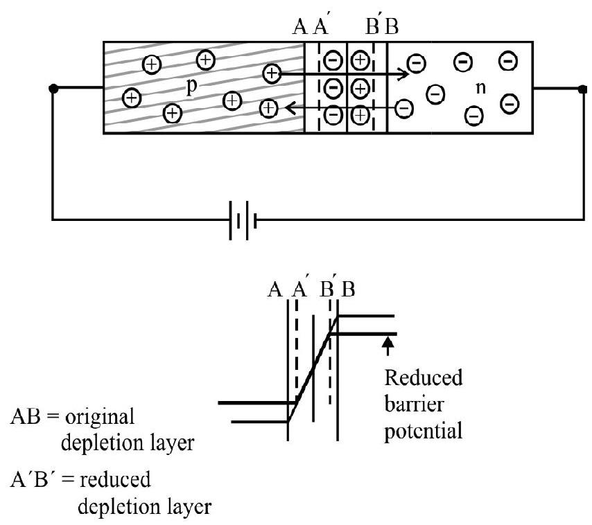
Fig. 12 (b)
If the applied voltage is small, the barrier potential will be reduced only slightly below the equilibrium
Hence in forward based junction, the applied electric field
Example-4:
A p-n junction diode is forward biased, what is the effect on the width of the depletion layer if the forward voltage is further increased?
Show Answer
Solution:
As the forward voltage ’
pn Junction diode under Reverse Bias
When a external voltage is applied across the diode in the direction of the inbuilt barrier potential
However, when the junction is reverse biased, a very small reverse current (uA) flows across the junction. This current is carried by few thermally generated minority carriers (electrons in
The current under reverse bias is essentially voltage independent upto a critical reverse bias voltage, known as breakdown voltage

Example-5:
Indicate which of the following

Show Answer
Solution:
a) R.B as p-side at lower potential
b) R.B as p-side at lower potential
c) F.B as p-side at higher potential
d) F.B as
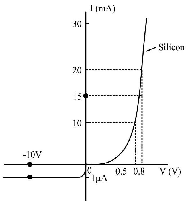
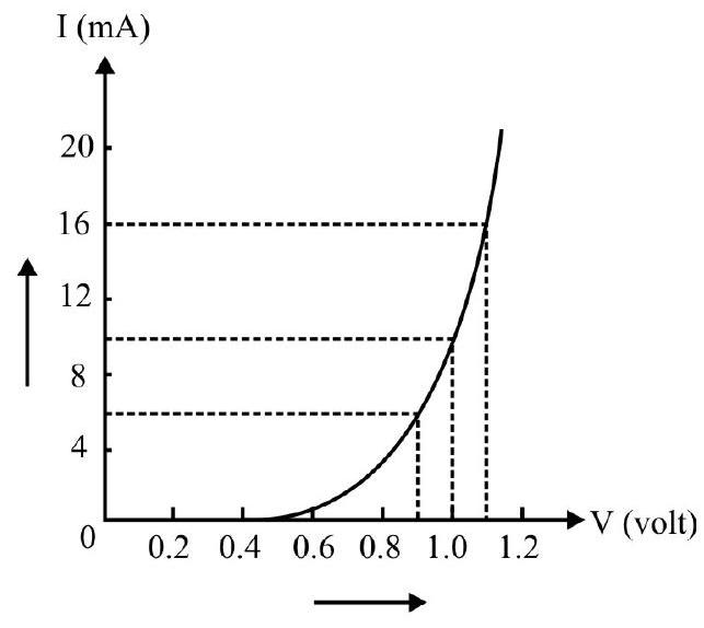
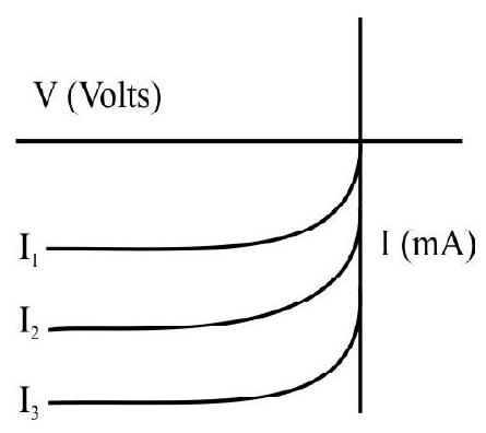
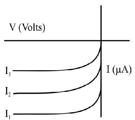
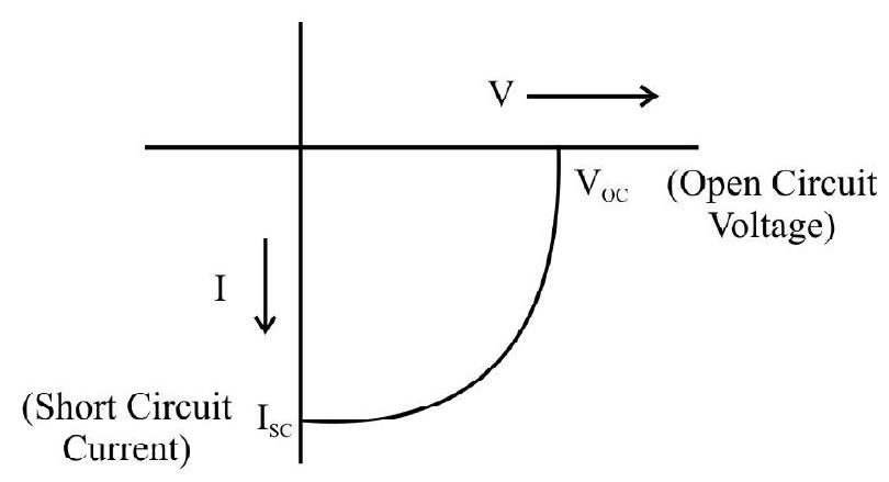
V-I Characterstatics of a Diode
The current voltage characterstic curve of a

The battery is connected to the diode through rehostat so that the applied voltage to the diode can be changed. For different values of V, the value of I is noted. Note that in forward bias measurement, we use milliammeter while we use microammeter in reverse bias, as current in reverse bias is significantly very small (due to drift of majority charge carriers).
As one can see in the graph above, the forward bias current increases very slowly, till the voltage across the diode crosses a certain value ’
For diode in reverse bias, the current is very small
Dynamic Resistance of a Junction Diode
The current voltage curve of a p-n junction diode shows that current does not vary linearly with voltage, that is ohm’s law is not obeyed. It is a non-linear device. In this case, we define, a quantity known as ‘dynamic resistance’ (or a.c. resistance) of
The dynamic resistance is not constant. It depends on the operating voltage.
Important Conclusion
The above discussion shows that
Example-6:
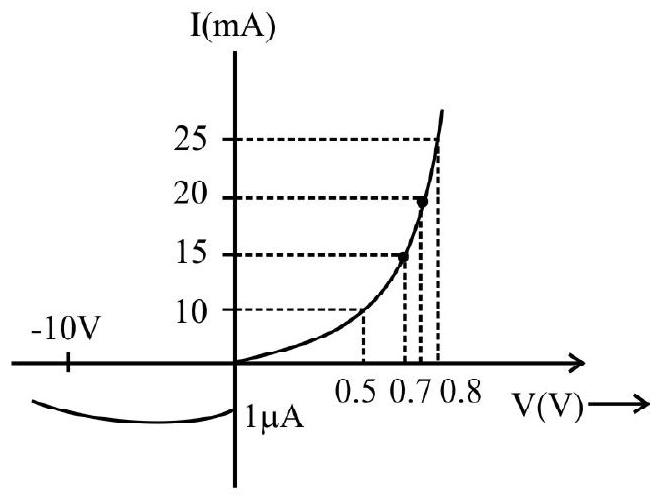
The V-I characteristic of a silicon diode is shown the fig. 14.17. Calculate the resistance of the diode at (a)
Show Answer
Solution:
Considering the diode characteristics as a straight line between
(a) From the cure, at
(b) From the curve at
Therefore,
Example-7:
When the voltage drop across a
Show Answer
Solution:
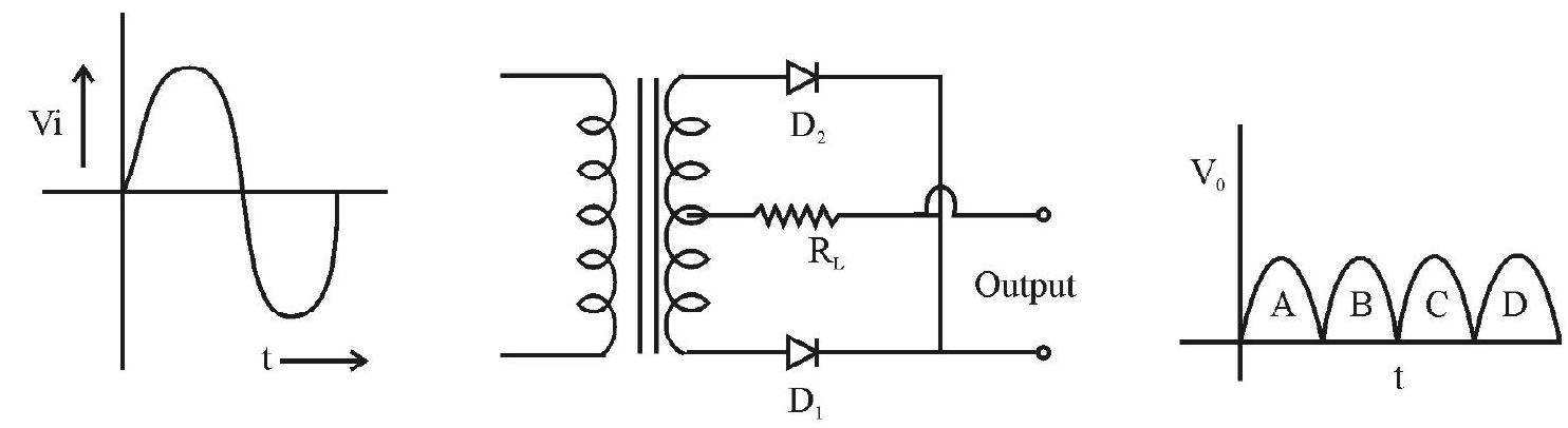
p-n Junction Diode as a Rectifier
Case-I: Half Wave Rectifier
From the V-I characterstic of a junction diode we known that is allows current to pass only when it is forward biased. So if an alternating voltage is applied across a diode the current flows only in that part of the cycle when the diode is forward biased. This property is used to rectify alternating voltages and the circuit used for this purpose is called a rectifier.
If an alternating voltage is applied across a diode in series with a load, a pulsating voltage will appear across the load only during the half cycles of the ac input during which the diode is forward biased. Such rectifier circuit, as shown in Fig. 17(a) is called a half-wave rectifier. The secondary of a transformer supplies the desired ac voltage across terminals
Therefore, in the positive half-cycle of ac there is a current through the load resistor

Case-II: Full-Wave Rectifier
The circuit using two diodes, shown in Fig. 18(a) gives output rectified voltage corresponding to both the positive as well as negative half of the ac cycle. Hence, it is known as full-wave rectifier. Here the p-side of the two diodes are connected to the ends of the secondary of the transformer. The n-side of the diodes are connected together and the output is taken between this common point of diodes and the midpoint of the secondary of the transformer. So for a full-wave rectifier the secondary of the transformer is provided with a centre tapping and so it is called centre-tap transformer. As can be seen from Fig. 18(b) the voltage rectified by each diode is only half the total secondary voltage. Each diode rectifies only for half the cycle, but the two diodes do so for alternate cycles. Thus, the output between their common terminals and the centre-tap of the transformer becomes a full-wave rectifier output.
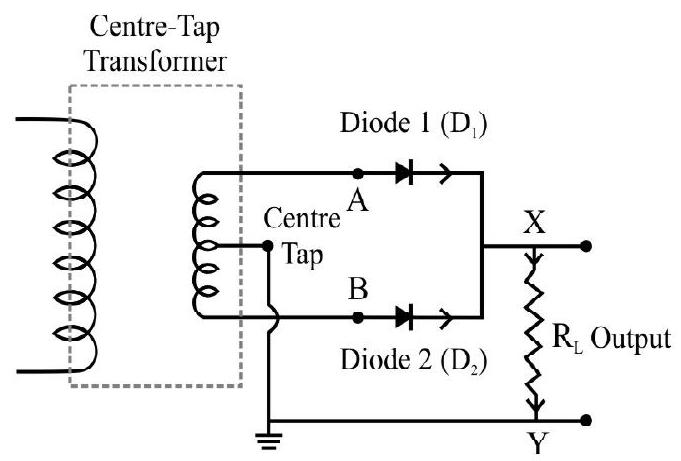
Fig. 18 (a): A full-wave rectifier circuit
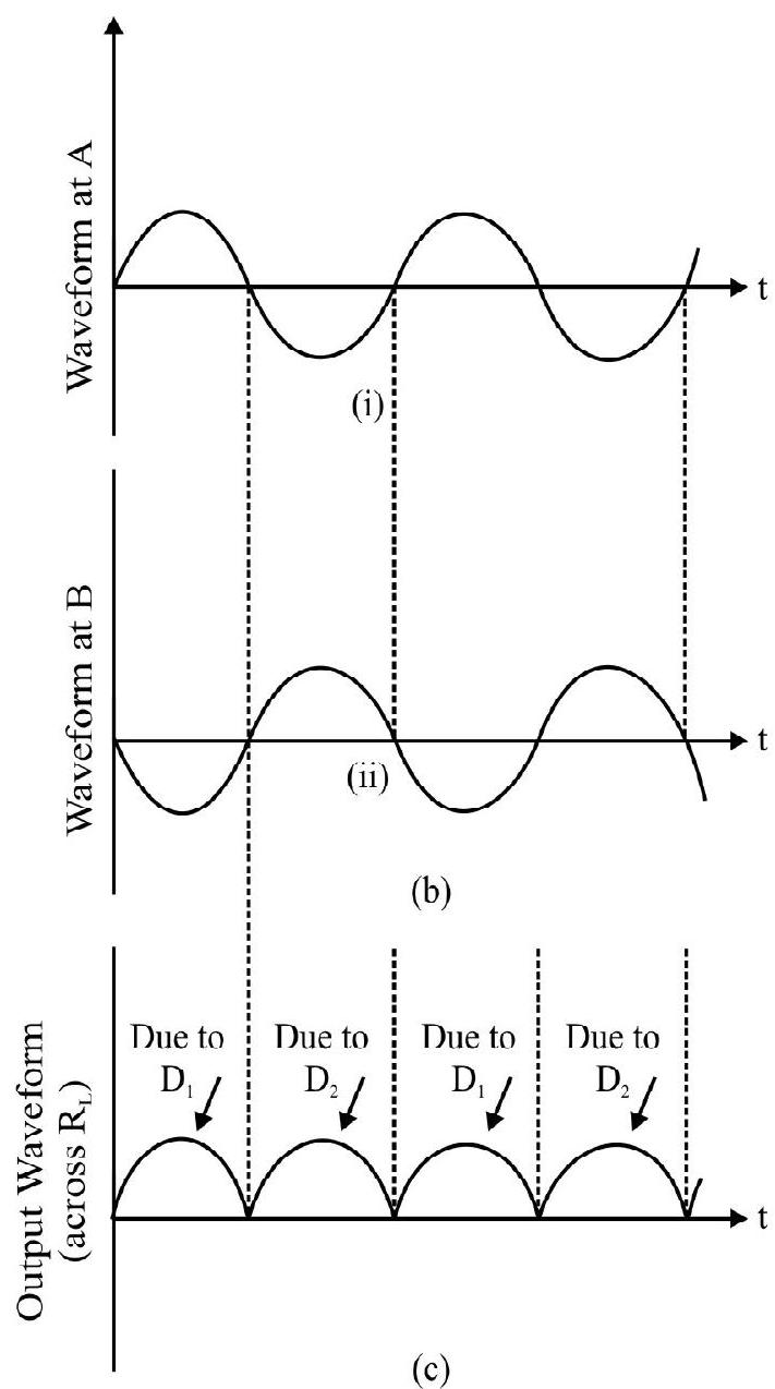
Fig. 18 (b): Input wave forms given to the diode
Example-8:
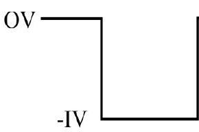
A square wave is applied to a
Show Answer
Solution:
The p-side of the diode is at zero potential (grounded). Therefore diode conducts only when negative half appears across the terminals (F.B) and does not conduct during positive half (R.B). Hence the output will be either
Special Purpose p-n Junction Diodes
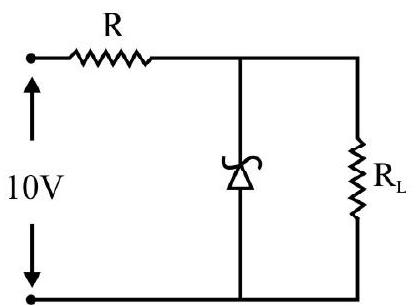
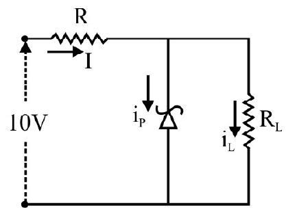
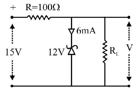
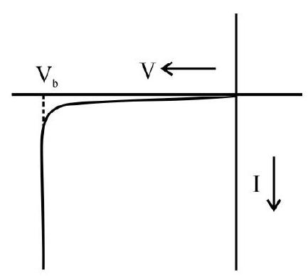
(i) Zener Diode
It is a voltage-regulating device based upon the phenomenon of avalanche breakdown in reverse biased
When the reverse bias voltage is increased, there is an abrupt rise in reverse saturation current. When the reverse bias voltage reaches a certain value, known as ‘breakdown’ or ‘zerner’ voltage. Thus, in this region of the curve, the voltage across the diode remains constant for very large range of currents. We can use this region for the purpose of voltage stablizer or regulator at a pre-determined value, (used this manner, it is known as ‘zener diode’).

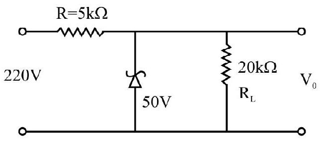
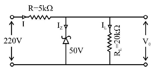
In the above circuit zener diode is selected with a zener voltage
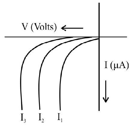
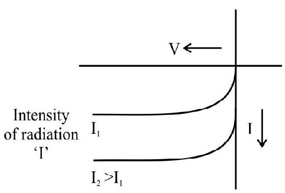
(ii) Photodiode
A photodiode is a special purpose

The magnitude of the photoelectric current depends on the intensity of the incident light (number of photons of light incident per second).
The
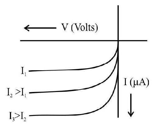
Fig. 20 (c)
I-V characterstic curves of a photodiode for different illumination intensities in reverse bias Fig. 20(c).
(iii) Light Emitting Diode
It is a heavily doped
When a
The semiconductors used for fabrication of visible LED’s must have a band gap of

I-V characterstic curve of a LED (similar to Si diode).
LED’s have following advantages over conventional in candescent lamps:
(a) low operational voltage and less power
(b) fast action and no warm up time required
(c) nearly monochromatic light
(d) fast on-off switching capability
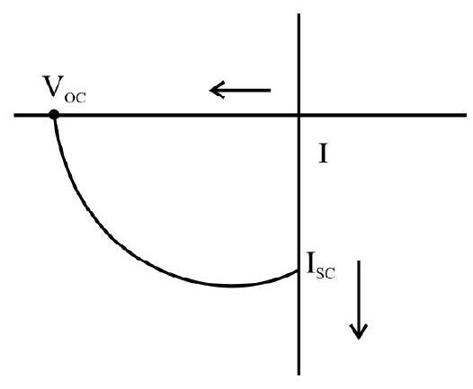
(v) Solar Cell
A solar cell is a
A p-Si wafer of about 300 um of
The generation of emf by a solar cell, when light falls on, it is due to the following three processes:
(a) Generation of electron-hole pair due to light (with photon energy
(b) Separation of electron and hole due to barrier field at the junction.
(c) Electron reaching the n-side collected by front contact and hole reaching the
Thus

Semiconductors with band gap close to
The solar cells are used to power electronic devices in satellites and space vehicles and also as power supply to some calculators.
The I-V characterstic curve of solar cell is drawn in the fourth quadrant of the co-ordinate exes. This is because a solar cell does not draw current but supplies the same to load as shown in Fig. 22(c).
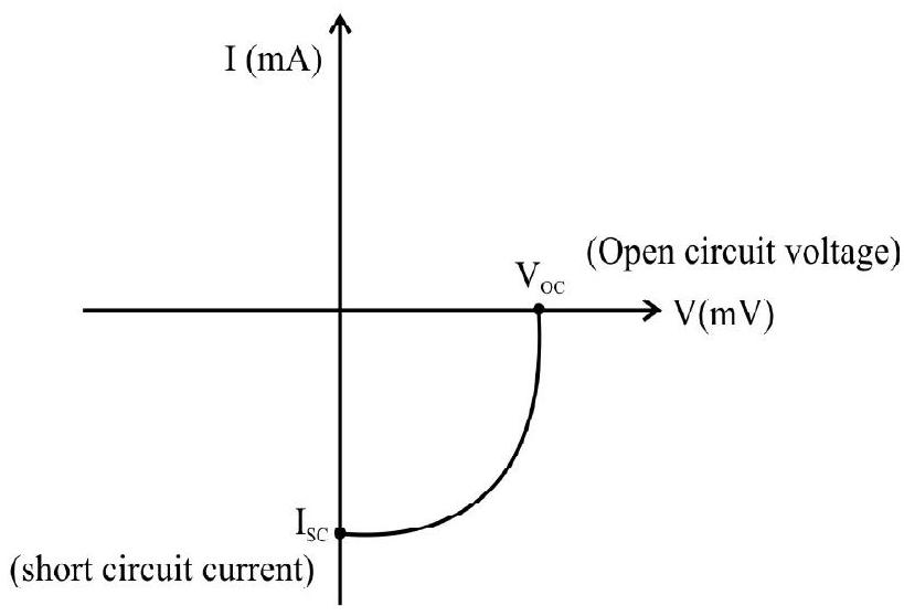
I-V characteristics of a solar cell
Fig. 22 (c)
Example-9:
In half wave rectification, what is the output frequency if the input frequency is
Show Answer
Solution:
(i)
(ii)
Example-10:
Ap-n photodiode is fabricated froma semiconductor with a band gap of
Show Answer
Solution:
Energy of photon
No, it can not detect a wavelength of
Example-11:
In case of
(a) Cut of voltage
(b) Knee voltage
(c) Critical voltage
(d) Zener voltage
Show Answer
Solution:
(d) Zener voltage
Example-12:
For detecting light intensity, we use
(a) Photodiode in reverse bias
(b) Zener diode in reverse bias
(c) LED in forward bias
(d) Solar cell
Show Answer
Solution:
(a) Photodiode in reverse bias
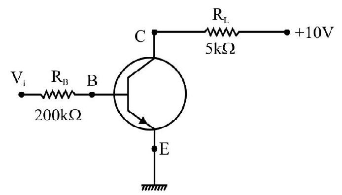
Junction Transistor
A transistor has three doped regions forming two
(i)

(ii) p-n-p Transsistor: Here two segments ofp-type semiconductor (turned as emitter and collector) are separated by a segment on

All the three segments in
Emitter: This segment of transistor is of moderate size and heavily doped. It supplies large number of majority charge carriers for the current flow through transistor.
Base: This is the central segment. It is very thin and lightly doped, as it controls the passage of charge carriers from emitter to collector. So that not more than
Collector: This segment collects a major position of the majority charge carriers supplied by the emitter. For this purpose, collector side is moderately doped and larger in size compared to emitter.
Transistor can be used two ways:
(i) Transistor as an amplifier and
(ii) As a switch
Depending upon its usage, biasing of transistor is done.
First we consider transistor ability to amplify the input signal (Amplification means strengthening the weak input a.c signal). For amplification, emitter base junction is forward biased and the base collector junction reverse biased.
Action of a Transistor
Under the forward bias, the majority charge carriers (electron in npn/holes in pnp) in emitters enter the base region in large numbers. The base in thin and lightly doped, most of majority charge carriers entering it pass on to the collector as it is reversed biased. A few of them recombine with minority at base as shown in the figure 23 (a) and (b).
It is intersting to note taht due to forward bias, a large current enters the emitter base junction, but most of it is diverted to adjacent reverse biased base-collector junction and the current coming out of the base becomes a very small fraction of the current that entered the junction.
The current entering into the emitter from outside in equal to the emitter current
where
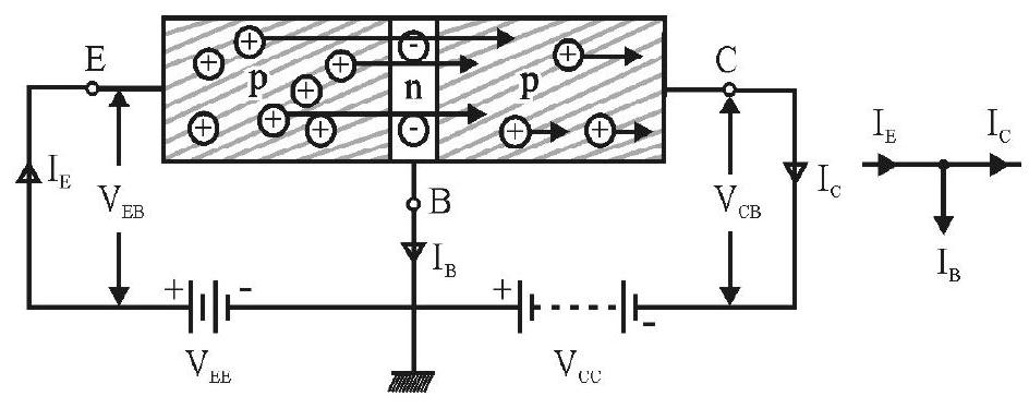
Fig. 23 (a): p-n-p transistor
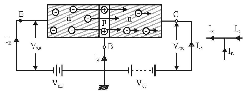
Fig. 23 (b): n-p-n transistor
Fig. 23: Transistor in “common-base configuration”
When the transistor is biased this way, emitter base junction forward biased and base-collector junction reverse biased it is said to be in active state.
The current gain
Since
The input resistance,
The output resistance
The input resistance
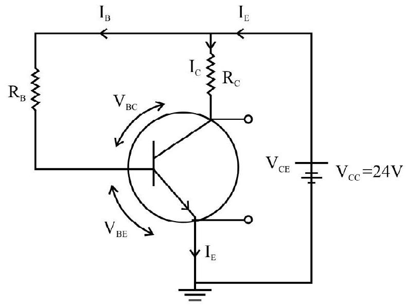
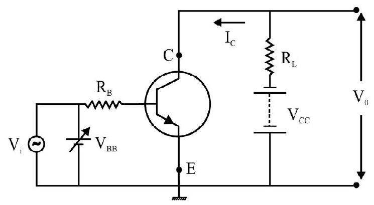
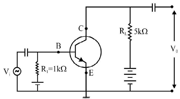
Transistor in Common-Emitter Configuration
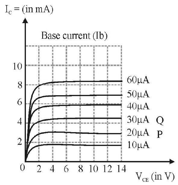
The graph showing the variation of current with voltage in a transistor is called transistor characterstics. The most widely used transistor is in common emitter configuration (CE).
When transistor is used in CE, congifuration, the input is between the base and emitter and output is between the collector and emitter. The circuit used to obtain the characterstics curves in shown in Fig. 24.
(i) Input Characterstics
A curve is plotted between the base current
We define a term called input resistance ’

Fig. 24: Circuit arrangement for studying the input and output characteristics of npn transistor in CE configuration
Input resistance
(ii) Ouput Characterstics
A curve is plotted between collector current

Output resistance - This is defined as the ratio of change in collector emitter voltage
The linear segment of output characterstics can be used to calculate this parameter.
(iii) Mutual or Transfer Characterstics Curve
If base voltage
The transconductance
Relation Between Transistor Parameters
By definition
and
Also
or
Rearranging we get

Fig. 25 (c) : Mutual or Transfer characteristics
Transistor as an Amplifier
For using the transistor as an amplifier, we use active region of the transistor as shown in Fig. 25(c). As amplifier is used to amplify small and weak alternating signals
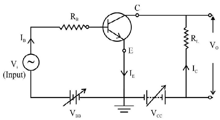
Fig. 26: Circuit arrangement for transistor as amplifier
First consider input a.c signal
and
As
That is change in
The change in
Hence voltage gain of the amplifier is
The negative sign represents that output voltage is opposite with phase with the imput voltage.
The power gain / amplification of a transistor is given as
It must be noted that transistor is not a power generating device. The energy for the higher a.c power at the output is supplied by the input battery
Transistor as an Oscillator
In the above discussion, we realize that an input a.c given to transistor appears as amplified output a.c signal. This means that an external input is necessary to sustain a.c signal in the ouput for an amplifier.
In an oscillator, we get an a.c output without any external input signal. In other words, an oscillator is a device that generates electric oscillations of constant amplitude and of a desired frequency, without any external inputs, the oscillations are self sustained.
To attain this, an amplifier is taken. A portion of the output power is returned back (feedback) to the input in same phase (positive feedback) with the starting power as shown in the Fig. 27 (a). The feedback can be achieved by inductive coupling (through mutual inductance) or LC or RC networks. Different types of oscillators essentially use different methods of coupling the output to input (feedback network). In the circuit given below Fig. 27(b) feedback is accomplished by inductive coupling from one coil (
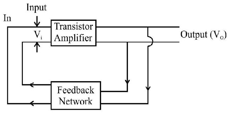
Fig. 27 (a) Principle of Oscillator
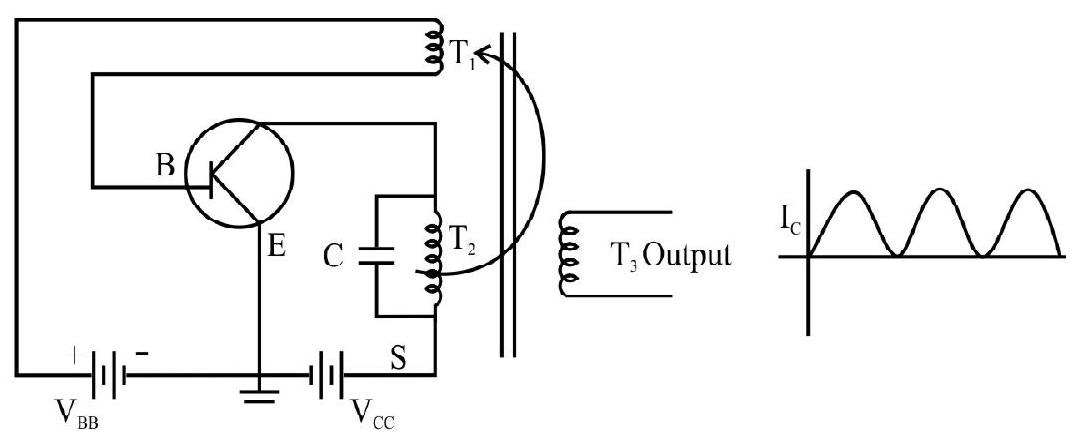
Fig. 27 (b) Circuit diagram of tuned collector oscillator
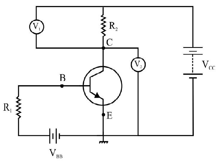
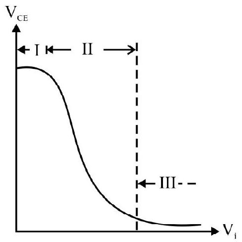
Transistor as a Switch
When the transistor is used in the cut off or saturation state it act as a swith as shown in the Fig. 25(c).
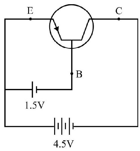
Let us try to analyse the behaviour of Si transistor as switch using
Hence
(Using Kirchoff’s law in output circuit,
When
We can conclude that as long as
Alternatively, we can say that a low input to transistor gives a high output and a high input gives a low output. The switching circuits are designed in a way that transistor does not remain in active state.
Example-13:
In a silicon transistor, a change of
Show Answer
Solution:
Given
As
Example-14:
The input resistance of transistor is
Show Answer
Solution:
Voltage gain
Analogue Circuits and Digital Circuits
There are two types of electronic circuits analogue circuits and digital circuits.
In analogue circuits, the voltage orcurrent varries continuously with time. Such a signal is called ‘analogue signal’. This is in the form of typical sinusoidal walleform.

In digital electronics we use only two levels are called digital signals. This signal is represented by pulse waveform or square waveform. In digital circuits only two values (represented by 0 and 1 ) of the input and output voltage are permissible.
Logic Gates
A gate is a digitcal circuit which follows certain logical relationship between input and output voltage. Therefore, they are generally known as ’logic gate’, gates because they central the flow of information. Logic gates are used in calculators, digital watches, computers, robots, industrial control system and telecommunication etc.
The five common logic gates used are OR, AND, NOT, NAND and NOR.
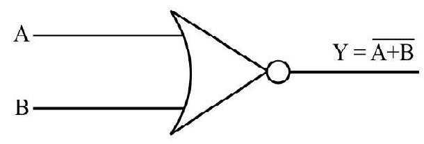
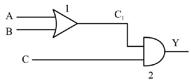
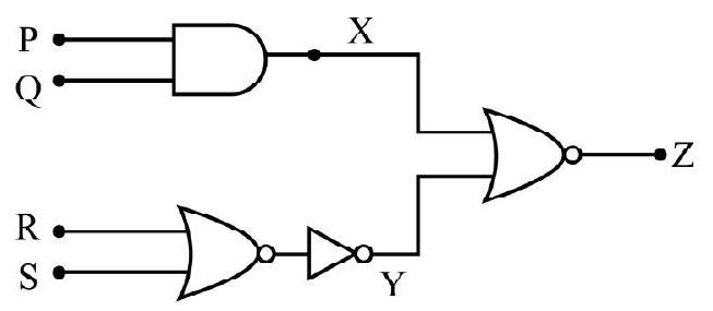
(i) OR Gate
An OR gate has two inputs related by one output. The truth table and logic symbol (circuit symbol) are shown below. The output
The Booliean representation of OR gate is
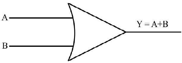
Logic Symbol
| 0 | 0 | 0 |
| 0 | 1 | 1 |
| 1 | 0 | 1 |
| 1 | 1 | 1 |
Truth table
Fig. 29: The Boleean representation of OR gate is
(ii) AND Gate
An AND gate has two inputs related by one output. The output
The Booliean representation of AND gate is
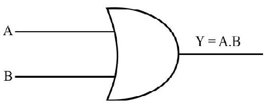
Logic Symbol
| 0 | 0 | 0 |
| 1 | 0 | 0 |
| 0 | 1 | 0 |
| 1 | 1 | 1 |
Truth table
Fig. 30: The Boleean representation of AND gate is
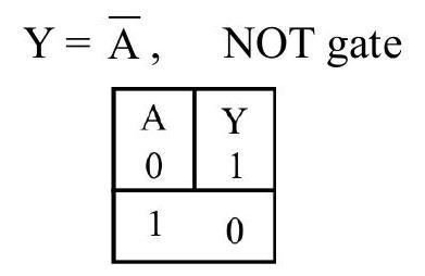
(iii) NOT Gate
This is the most basic gate with one input related to one output. It gives inverted version of input voltage as output voltage. This is the reason it is also known as inverter. The logic symbol and truth table are given as below:
The Booliean representation of NOT gate is
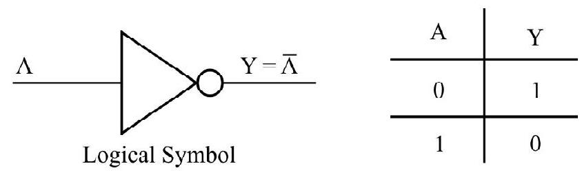
Truth table
Fig. 31 : The Boleean representation of NOT gate is
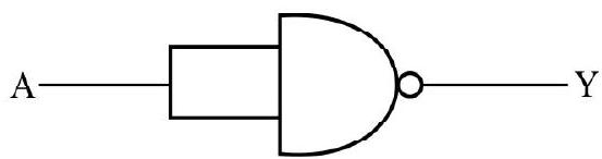
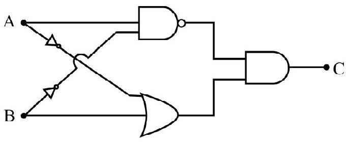
(iv) NAND Gate
This is an AND gate followed by a NOTgate as shown in Fig. 32. If the inputs
NAND gates are also called universal gates since by using these gates we can realize other basic gates like OR, AND and NOT. The logic symbol and truth table are given below:
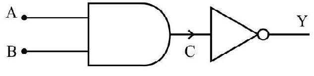
Fig. 32
The Booliean representation of NAND gate is
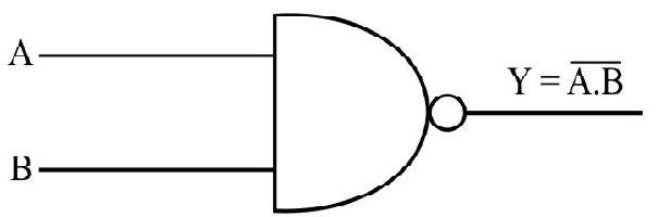
Logic Symbol
| 0 | 0 | 1 |
| 0 | 1 | 1 |
| 1 | 0 | 1 |
| 1 | 1 | 0 |
Truth table
Fig. 33: The Boleean representation of NAND gate is
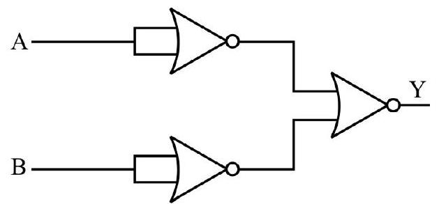
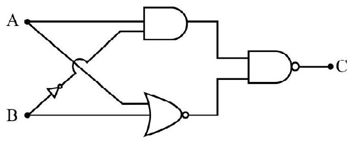
(v) NOR Gate
This is an OR gate followed by a NOT gate as shown in Fig. 34. Its output
Thelogic symbol and truth table are given below:
The Booliean representation of NOR gate is
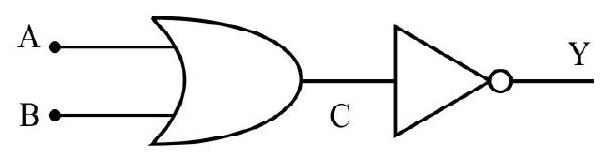
Fig. 34
Logic Symbol
| 0 | 0 | 1 |
| 0 | 1 | 0 |
| 1 | 0 | 0 |
| 1 | 1 | 0 |
Truth table
Fig. 35: The Boleean representation of NOR gate is
Example-15:
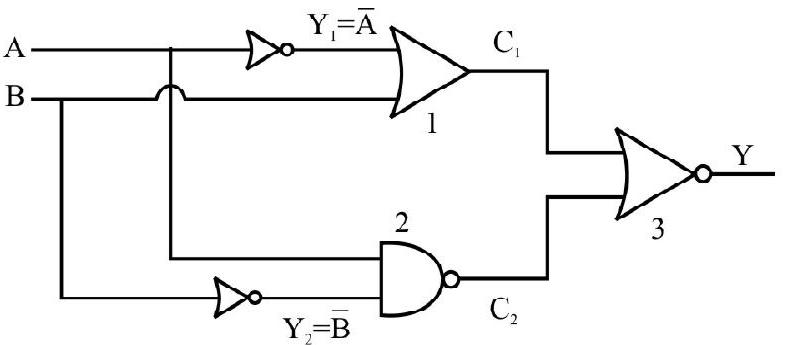
Write the truth table for a NAND gate connected as given in figure.
Show Answer
Solution:
The above operation represent one input connected to one output through NOT gate.
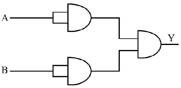
Example-16:
The output of an OR gate is connected to both the inputs of a NAND gate. Draw the logic circuit of this combination and the truth table.
Show Answer
Solution:
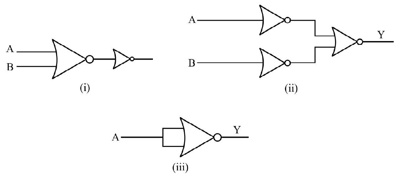
When two inputs of NAND are joined together, it works as NOT gates. The OR gate connected to NOT gate results in NOR gate.
| 0 | 0 | 0 | 1 |
| 1 | 0 | 1 | 0 |
| 0 | 1 | 1 | 0 |
| 1 | 1 | 1 | 0 |
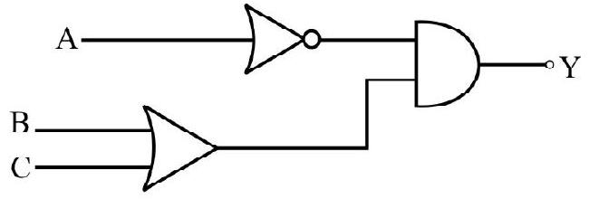
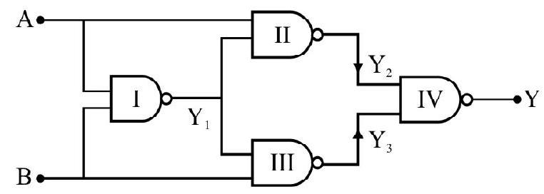
Example-17:
Write the truth table for the following combination of gates.
Show Answer
Solution:
| 0 | 0 | 0 | 1 |
| 1 | 0 | 1 | 0 |
| 0 | 1 | 1 | 1 |
| 1 | 1 | 1 | 0 |
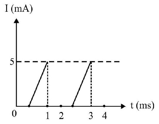
Example-18:
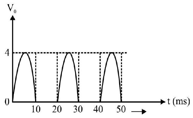
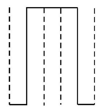
Justify the output waveform
Show Answer
Solution:
Note the following:
At
For
For
For
For
For
For

Therefore the waveform
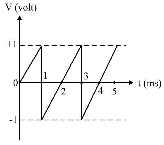
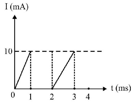
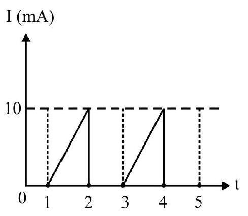
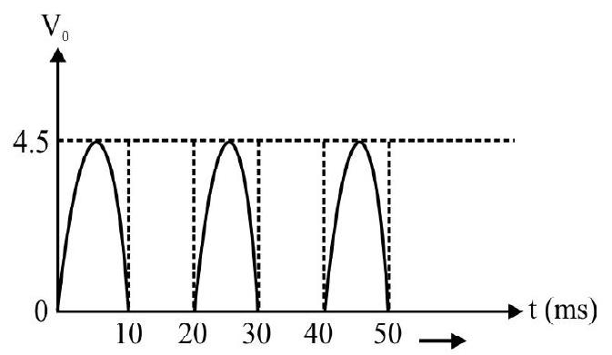
Example-19:
Sketch the output wavelength
Show Answer
Solution:
Example-20:
Why are NAND and NOR gates called digital building blocks?
Show Answer
Solution:
The repeated use of NAND or NOR gate can produce all the three basic gates (OR AND and NOT) whose different combinations provide us large number of digital circuits. Hence NAND and NOR are called digital building blocks.
PROBLEMS FOR PRACTICE
1. A sample of pure Ge has a hole density of
Show Answer
[Answer:2. The electrical conductivity of a semiconductor increases when radiation of wavelength shorter than
Show Answer
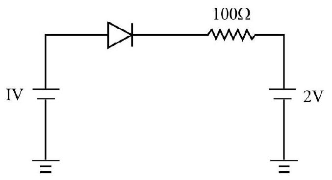
[Answer:3. When the voltage drop across a
Show Answer
[Answer:4. A square wave as shown below is applied to a  5. In a p-n junction diode, the current I can be expressed as:
where
(i) Find the forward current at forward voltage
(ii) What will be the increase in current if voltage across the diode is increased to
(iii) What is the dynamic resistance?
Show Answer
[Answer: (i)6. The circuit given below shows two diodes each with a forward bias resistance of
Show Answer
[Answer:7. The V-I characterstics of silicon diode are shown above. Calculate the diode resistance at
Show Answer
[Answer:8. In a common emitter amlifier an increase of
Show Answer
[Answer:9. In a npn transistor
Show Answer
[Answer: 49]10. An npn transistor is connected in common emitter configuration in which collector supply is
Show Answer
[Answer:11. In the given circuit below,
Find
Show Answer
[Answer:12. Write the truth table for the following combination of gates.
[Answer: ]
13. Write the truth table for the following circuit. Identify the logic operation performed.
[Answer: ]
14. Two amplifiers are connected one after other in series. The first amplifier has a voltage gain of 10 and second has voltage gain of 20 . If the input signal is
Show Answer
[Answer: 2V]15. Out of the following combinations of gates given, identify the circuit, which performs the logic operation ‘AND’.
Show Answer
[Answer: (ii)]Question Bank
Key Learning Points
1. The large number of energy levels confined in a small region of energy range of a given solid, consitute, a band known as ‘Energy Band’.
2. The upper energy levels are called conduction band and lower energy levels are called valence band.
3. In some solids, there is an energy gap in between conduction band and valence band; known as forbiddengap.
4. In metals, the conduction band and valence band partly overlap each other and there is no forbidden gap.
5. In isulators, forbidden gap is quite large
6. In semiconductor, the forbidden gap is small ( 1 to
7. A pure semiconductor which is free from every impurity is called intrinsic semiconductor. In intrinsic semiconductor
8. The process of delibrate addition of a desirable impurity to a pure semiconductor to modify its conductivity in a controlled manner; is called dopoing. The semiconductor so obtained is called extrinsic semiconductor. The impurity atoms added are called dopants.
9. When a pure semiconductor of Ge or
10. When a pure semiconductor of
11. Energy band diagram for extrinsic semiconductor is modified. In n-type, there is additional donor level just below conductor band and in p-type there is additional acceptor level just above valence band.
12. The electrical conductivity of a semiconductor crystal is given by
13. When a semiconductor is heated, its resistance decreases, specific resistance decreases and electrical conductivity increases.
14. A thin layer formed on both sides of the
15. The potential barrier or electric field set up across the junction depends upon the amount of doping of the semiconductor crystal and temperature.
16. During forward bias (
17. During reverse bias (
18. Voltage drop across the
19. The potential barrier at
20. An ideal p-n junction diode has unidirectional property. It conducts only in one direction, when forward biased.
21. The ratio of change in applied (junction) voltage
22. The unidirectional property of an ideal
23. In
24. In
25. There are special purpose
26. Zener diode is just like an ordinary
27. Photodiodes are the special type of diodes working in a reverse bias. These diodes work on the principle that change in the intensity of radiation results in change in reverse saturation current. For
this to happen, energy of incident photon must be greater than or equal to the barrier energy of the semiconductor. The photodiodes can be used as a photodector to detect optical signal.
28. Solar cell is a device in which light energy is converted into electrical energy. Semiconductors with band gap close to
29. Light emitting diode, commonly known as ‘LED’ is a heavily doped
30. A junction transistor is a semiconductor device which obtained by growing a thinlayer of one type of semiconductor in between the two thick layers of other type of semiconductor. The most common configuration are pnp and npn transistor.
31. The junction transistor has three segments-emitter, base and collector. The function of emitter is to emit the majority charge carriers. Function of collector is to collect the majority charge carriers and base provides the proper bias for the collection of charge carriers.
32. The base region is very thin and lightly doped. The emitter is heavily doped.
33. During the action/working of a transistor.
where
34. The transistor can be used as an amplifier in CE configuration. During amplification, input and output signal are
35. Current gain in CE configuration is given by
36. Current gain in common base configuration is
37. A.C voltage gain in CE amplifier is given by
38. A.C power gain in
39. In the transistor as an oscillator, a positive feedback is provided from on output tank circuit (LC) to the input circuit (transistor as amplifier) to obtain the sustain oscillations with constant amplitude. Hence oscillator is an amplifier with positive feedback.
40. Transistor is used as an amplifier only in active state. That is emitter base junction forward bias and base emitter junction reverse bias.
41. Transistor can be used as a switch in the cutoff or saturation state.
42. There are some special circuits which handle the digital data consisting of 0 and 1 levels. This forms digital circuits.
43. The digital circuit having logic relationship between input and output signal are called ’logic gates’.
44. The important basic logic gates are OR, AND, NOT, NAND and NOR gates.
45. NAND and NOR gates are considered as universal gates as these gates are building blocks of OR, AND and NOT gates.
Average
Semiconductors
1. Semiconductors are fourth group elements in periodic table. Silicon (Si), Carbon (C) and Germanium (Ge) att are fourth group elements in periodic talbe. Which of the following statement is correct?
(1) All are semiconductors
(2) Only Si and Ge are semiconductors
(3) Only carbon is semiconductor
(4) Carbon (C) and Germanium are semiconductors
Show Answer
Correct answer: (2)
Solution:
Only Si and Ge are semiconductors carbon is an insulator. The energy gap for Si and Ge is nearly
Difficult
Semiconductors
2. Most of currently available semiconductor are elemental semiconductors
(1) (a) GaAs (b) CdSe (c) anthracene
(2) (a) GaAs (b) anthracene (c) polyanline
(3) (a) anthracene (b) GaAs (c) polyanline
(4) (a) CdSe (b) polyanline (a) anthracene
Show Answer
Correct answer: (2)
Solution:
Factual knowledge.
Easy
Semiconductors
3. A “Hole” in a semiconductor is produced when an electron breaks away from a covalent bond in a semiconductors. Which of the following statements regarding a hole is incorrect?
(1) A hole has same magnitude of charge as on an electron
(2) In an external eletric field a hole moves in a direction opposite to that of free electron
(3) The energy of a hole is less as compared to that of an electron
(4) In same external applied electric field the drift speed accquired by a hole is less than the drift speed accquired by a free electron
Show Answer
Correct answer: (3)
Solution:
The energy of hole is less than the energy of an electron.
Easy
Semiconductors
4. An intrinsic semiconductor is at a temperature of
(1) does not vary as temeperature rises to
(2) decreases linearly with rise in temperature
(3) increases exponentially as the energy gap increases
(4) decreases exponentially as the energy gap increases
Show Answer
Correct answer: (4)
Solution:
As energy gap increases the probability of electron jump from conduction to valency band decreases exponentially.
Easy
Semiconductors
5. An electric field of
(1)
(2)
(3)
(4)
Show Answer
Correct answer: (3)
Solution:
Velocity of the carriers
Velocity is also given by,
Mobility
Average
Conductivity of Semiconductors
6. Mobilities of electrons and holes in a sample of intransic germanium at room temperature are
(1)
(2)
(3)
(4)
Show Answer
Correct answer: (3)
Solution:
The conductivity of a semiconductive in terms of number density and mobility is
where
Easy
Extrinsic Semiconductors
7. The impurity atoms with which pure silicon should be doped to make a n-type semiconductor are those
(1) Boron
(2) Indium
(3) Antomony
(4) Aluminium
Show Answer
Correct answer: (3)
Solution:
As n-type semiconductor is obtained by adding pentavalent impurity atom. Hence impurity should be of antomony out of all the four choices given.
Average
Semiconductors
8. For the same dopant concentration, the n–type silicon semiconductor has _____________ as compared to a p-type silicon semiconductor.
(1) Higher conductivity
(2) Higher resistivity
(3) Lower mobility
(4) Lower net charge
Show Answer
Correct answer: (1)
Solution:
For the silicon semiconductor,
Mobility of electrons
Mobility of holes
Conductivity of electrons
Conductivity of holes
Now, since dopant concentration is same,
Concentration of electrons
Conductivity of n-type sample is more than
Average
Semiconductors
9. At thermal equilibrium, the concentration of majority carriers in an n-type extrinsic semiconductor, is
(1) Inversely proportional to the intrinsic carrier concentration
(2) Directly proportional to the intrinsic carrier concentration
(3) Inversely proportional to the majority carrier concentration
(4) Directly proportional to the majority carrier concentration
Show Answer
Correct answer: (3)
Solution:
If
or
Average
Semiconductors
10. In a p-type semiconductor, the concentration ofholes is
(1)
(2)
(3)
(4)
Show Answer
Correct answer: (2)
Solution:
If
Average
Semiconductors
11. A silicon sample is uniformly doped with
(1) n-type with carrier concentration of
(2) p-type with carrier concentration of
(3) n-type with carrier concentration of
(4) p-type with carrier concentration of
Show Answer
Correct answer: (1)
Solution:
Phosphorous is pentavalent impurity and will make the silicon sample n-type. Since the donor atoms are fully ionized.
Number of electrons
Indium is trivalent impurity and will make the silicon sample p-type. Since the acceptor atoms are fully ionized.
Number of holes
Therefore, the sample will be n-type and the net carrier concentration will be
Average
Semiconductors
12. In an intrinsic semiconductors number density of electrons and holes is same and is
(1) Increase in conductivity is due to increase in n only
(2) Increase in conductivity is due to increase in relaxation time
(3) The increase in
(4)
Show Answer
Correct answer: (4)
Solution:
Facturial knowledge about semiconductors.
Easy
Semiconductors
13. Pure Si and
(1) n-type; with electron concentration of
(2) p-type; with electron concentration of
(3) n-type; with electron concentration of
(4) p-type; with electron concentration of
Show Answer
Correct answer: (4)
Solution:
Given ne
Let
Since
Average
Semiconductors
14. A pure siliconn sample has
(a)
(b)
one by one. What is ratio of resistivity of doped sample in (a) and (b) due to majority charge carriers? Given:
Mobility of electrons
(1) 1
(2) 2
(3)
(4)
Show Answer
Correct answer: (4)
Solution:
(a) The majority charge carriers are electrons.
(b) The majority charge carriers are holes
Difficult
Semiconductors
15. A pure silicon semiconductor has a size of
(1)
(2)
(3)
(4)
Show Answer
Correct answer: (4)
Solution:
Volume of given sample
The extent of doping of assenic is more than that of indium.
The net extent of doping
The number of electrons in given sample
The numbe of holes in given sample
Average
Semiconductors
16. A pure germanium rod has a radius of
(1)
(2)
(3)
(4)
Show Answer
Correct answer: (3)
Solution:
The electric field in
Let
The current,
Given
Similarly the current
The total current
Easy
Semiconductors
17. In a semiconductor doped with phospohrous the Fermi-level is
(1)
(2)
(3)
(4)
Show Answer
Correct answer: (2)
Solution:
The doped semiconductive is a n-type semiconductor. The position of Fermi-level below conduction band is inversly proportional to the temperature of material on Kelvin scale. Given
Now,
Average
Junction Diode
18. The barrier potential of a
(a) type of semiconductor
(b) amount of doping
(c) temperature.
Which one of the followings is correct?
(1) (a) and (b) only
(2) (b) only
(3) (b) and (c) only
(4) (a), (b) and (c)
Show Answer
Correct answer: (4)
Solution:
Factual knowledge about junction diode.
Easy
19. The width of depletion region in a p-n junction diode is
(1)
(2)
(3)
(4)
Show Answer
Correct answer: (1)
Solution:
Let
Difficult
20. A potential barrier of
(1)
(2)
(3)
(4)
Show Answer
Correct answer: (2)
Solution:
In a junction diode; due to depeltion layer p-region is at a lower potential than n-region. The electron enters depletion layer from
where
On solving we get
Difficult
21. In a p-n junction a potential barrier of
(1)
(2)
(3)
(4)
Show Answer
Correct answer: (1)
Solution:
The p-region is at a lower potential than
When hole crosses depletion layer from
The correction choice is (1)
Difficult
22. In a p-n junction there exists a barrier potential. Fig. (a) shows the three barrier potential of a p-n junction marked as I, II and III.

Fig. (b) shows a junction diode biased as.

The correct commbination of biasing and barrier potential is
(1) I and IV; II and V; III and VI
(2) II and IV; III and V; I and VI
(3) I and V; II and VI; III and IV
(4) I and VI; II and V; III and IV
Show Answer
Correct answer: (2)
Solution:
I and II and III show barrier potential of an unbiased; forward biased and reverse biased junction diode respectively. In Fig. (b); IV is a forward biased; V is a reverse biased and VI is forward biased; V is a reverse biased and
Average
Diode
23. In a junction diode the current is zero if applied forward bias voltage is
(1)
(2)
(3)
(4)
Show Answer
Correct answer: (3)
Solution:
Let
Also
The current in junction diode; in forward bias is zero is applied p.d is less than or equal to junction potential.
Difficult
Diode
24. In a junction diode
(1)
(2)
(3)
(4)
Show Answer
Correct answer: (3)
Solution:
The current I; in general; in a junction diode is
Under forward bias conditions
Under reverse bias conditions for high value of V;
Average
25. For a p-n junction diode which of the following statement is correct
(1) In forward biasing there is a diffusion and in reverse bias there is drifting of charge carriers across the junction.
(2) In forward bias there is drifting and in reverse bias there is diffusion of charge carriers across the junction.
(3) In both forward and reverse biasing the current is due to diffusion of charge carriers across the junction.
(4) In both forward and reverse bias there is current due to drifting of charge carriers across the junction.
Show Answer
Correct answer: (1)
Solution:
Factual knowledge about moment of charge carriers in a p-n junction diode.
Average
p–n Junction Diode
26. The current through an ideal
(1) zero
(2)
(3)
(4)
Show Answer
Correct answer: (1)
Solution:
As
Average
p–n Junction Diode
27. In the circuit diagram shown below; the potential difference between the pionts

(1)
(2)
(3)
(4)
Show Answer
Correct answer: (4)
Solution:
As the diode is in reversebias, (
Difficult
Diode
28. In Fig. (a) the forward bias ideal diode is D. The applied voltage at anode varies with time as shwon in FIg. (b). The variation of current in circuit as a function of time is (knee voltage of diode

(a)
(b)
(1)
(2)
(3)
(4)
Show Answer
Correct answer: (1)
Solution:
From 0 to
In time interval
Average
Diode
29. Fig. shows forward bias characterstics of a junction diode. The knee voltage and resistance of dide are:
(1)
(2)
(3)
(4)
Show Answer
Correct answer: (2)
Solution:
The knee voltage of diode
Consider points
The resistance of diode
Average
p–n Junction Diode
30. In the circuit given below, the value of the current is
(1) Zero
(2)
(3)
(4)
Show Answer
Correct answer: (2)
Solution:
As
The forward current
Average
Semiconductor Diode
31. A silicon
(1)
(2)
(3)
(4)
Show Answer
Correct answer: (4)
Solution:
For a silicon pn junction, for every
Average
p–n Junction Diode
32. In the given circuit, the junction diodes are ideal. The current through battery is
(1)
(2)
(3)
(4)
Show Answer
Correct answer: (2)
Solution:
In circuit,
The current drawn from battery
Difficult
p–n Junction Diode
33. In the circuit given below, the junction diode
(1)
(2)
(3)
(4)
Show Answer
Correct answer: (1)
Solution:
As junction diode is reverse biased, it offers infinite resistance in the circuit. Due to it, the current in the circuit is zero. Therefore p.d across
Difficult
Diode
34.

Fig. (a) shows a “black-box” with three connecting terminals P, Q and R. Three components two diodes and one resistance is connected across the three terminals in same unknown arrangement. Fig. (b) shows black-box connected as shown in circuit. In I vs V graph obtained when
(1)
(2)
(3)
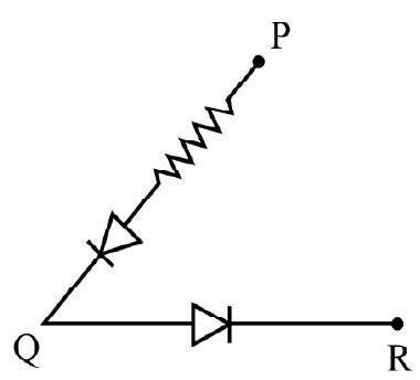
(4)
Show Answer
Correct answer: (1)
Solution:
The characterstics curve shown in Fig. (c) is forward bias characterstic of a diode with a knee voltage of
Hence correct answer is (1).
Average
Zener Diode
35. For a zener diode; which of the following statements is correct?
(1) n region is heavily doped only
(2) p region is heavily doped only
(3) Both n- and p-region is heavily doped
(4) A zener diode in a working circuit is always forward biased
Show Answer
Correct answer: (3)
Solution:
In a zener diode both
For proper working in any circuit zener diode is always reverse biased.
Difficult
Zener Diode
36. From the zener diode circuit shown in the figure given below, the current through zener is
(1)
(2)
(3)
(4)
Show Answer
Correct answer: (3)
Solution:
Given,
From Kirchoff’s current law,
Average
p–n Junction DIode
37. Silicon diode has a barrier potential of
(1)
(2)
(3)
(4)
Show Answer
Correct answer: (1)
Solution:
Both the Si diodes are in F.B and are in parallel.
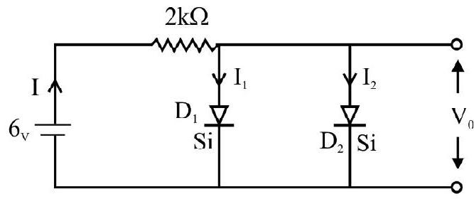
Hence
Current
Average
LED
38. For a Light-Emitting-Diode (LED) which of following statements is wrong?
(1) It is a heavily doped
(2) When forward biased the concentration of minority charge carriers increases rapidly on the sides of the junction boundary
(3) The energy released due to recommbination of electrons and holes is mostly transferred into the thermal energy of lattice vibrations
(4) LED emits light when it is reverse biased
Show Answer
Correct answer: (4)
Solution:
LED emitts light when it is forward biased. As forward current increases intensity of light emitted by LED also increases. When LED is reverse biased it emits no light. The LED is damaged when it is reverse biased.
Difficult
Diode
39.

Fig. (a) shows a half-wave rectifier. Fib. (b) is the
(1)
(2)
(3)
(4)
Show Answer
Correct answer: (3)
Solution:
The knee voltage of given diode, from Fig. (b) is
The correct output is given in (3).
Average
40. A full wave rectifier circuit alongwith the output is shown in the figure. The contribution from diode ’ 1 ’ is
(1) C, D
(2) A, C
(3) B, D
(4) A, D
Show Answer
Correct answer: (3)
Solution:
At
Average
Diode
41. An a.c voltage of peak value
(1)
(2)
(3)
(4)
Show Answer
Correct answer: (2)
Solution:
Barrier potential of silicon diode
Peak current through the diode in the circuit
Peak output voltage
Difficult
Zener Diode
42. In the circuit shown inFig. the breakdown voltage and current of zener diode is
(1)
(2)
(3)
(4)
Show Answer
Correct answer: (1)
Solution:
In Fig.
The zener voltage drop
Therefore
Obviously,
Also,
Difficult
Zener Diode
43. In the circuit shown in Fig. the zener diode draws a current of
(1)
(2)
(3)
(4)
Show Answer
Correct answer: (3)
Solution:
In loop ABEF; p.d across zener diode
The current, I; as shown in Fig.; is
At branch point B; current I divides,
Since zener diode is rated as
Average
Diode
44. In Fig. shown
(1) 1
(2) 2
(3)
(4)
Show Answer
Correct answer: (2)
Solution:
When
When
Difficult
Diode
45. In Fig. shown
(1)
(2)
(3)
(4)
Show Answer
Correct answer: (2)
Solution:
Diode
Average
LED
46. The semiconductor used for fabrication of visible LEDs must atleast have a band gap of
(1)
(2)
(3)
(4)
Show Answer
Correct answer: (2)
Solution:
Spectral range of visible light is from
Average
Photodiode
47. I-V characterstics of a photodiode for different illumination intensity
(1)
(2)
(3)
(4)
Show Answer
Correct answer: (1)
Solution:
In photodiode, change in the current is directly proportional to the change in the light intensity. It is operated in reverse bias.
Average
Solar Cell
48. The
(1)
(2)
(3)
(4)
Show Answer
Correct answer: (2)
Solution:
I-V characterstics of a solar cell is drawn in the fourth quadrant of the coordinate axes. This is shown in Fig. (2).
Average
LED
49. Intensity of light emitted by LED depends on
(1) Forward bias voltage
(2) Forward current
(3) Forward resistance
(4) Nature of semiconductor crystal
Show Answer
Correct answer: (2)
Solution:
Intensity of light emitted by LED depended on the forward current flowing in LED, with increase in forward current, intensity of light emitted increases.
Average
LED
50. Colour of the light emitted by LED depends on
(1) Forward bias voltage
(2) Reverse bias voltage
(3) Nature of semiconductor crystal
(4) Forward resistance
Show Answer
Correct answer: (3)
Solution:
Colour of the light emitted by LED depends on the energy gap of the semiconductor crystal. Hence the nature of the semiconductor crystal.
Easy
Semiconductors
51. Fig. shows V-I characterstic for a semiconductor device. Which of the following statements is correct?

(1) It is V-I characterstics of a solar cell, where point A represents open circuit voltage and point B short circuit current
(2) It is a solar cell and points A and B represent open circuit voltage and current respectively
(3) It is a photodiode and points A and B represent open circuit voltage and current respectively
(4) It is a LED and points A and B represent open circuit voltage and short circuit current respectively
Show Answer
Correct answer: (1)
Solution:
The given graph is
Easy
Transistor
52. If
(1)
(2)
(3)
(4)
Show Answer
Correct answer: (1)
Solution:
In a transistor area of collector
Easy
Transistor
53. In Fig. shown what is nature of biasing of emitter and collector. What is
(1) E-forward biased, C-reverse biased,
(2) E-forward biased, C-forward biased,
(3) E-reverse biased, C-reverse biased,
(4) E-forward biased, C-forward biased,
Show Answer
Correct answer: (1)
Solution:
In the emitter base loop there is battery of p.d
The collector
Average
Junction Transistor
54. In a junction transistor, the current gain in
(1) 99
(2) 198
(3) 495
(4) 594
Show Answer
Correct answer: (3)
Solution:
Av, voltage gain in CE configuration
As given
Average
Electronic Devices
55. In a
(1) Emitter current will be
(2) Emitter current will be
(3) Emitter current will be
(4) Emitter current will be
Show Answer
Correct answer: (2)
Solution:
Easy
Junction Transistor
56. In a transistor the current amplification ’
(1)
(2)
(3)
(4)
Show Answer
Correct answer: (4)
Solution:
By definition, current gain
Also,
Therefore
Average
Transistor
57. Is an
(1) 2
(2) 3
(3) 4
(4) 5
Show Answer
Correct answer: (4)
Solution:
Average
Transistor
58. Fig. shows common-emitter characterstic curve of a transistor. For
(1)
(2)
(3)
(4)
Show Answer
Correct answer: (3)
Solution:
The current gain;
For
We know
Average
Junction Transistor
59. The transfer ratio
(1)
(2)
(3)
(4)
Show Answer
Correct answer: (4)
Solution:
Given
as
From Eqns. (1) and (2) we have
Average
Electronic Devices
60. A signal of
(1)
(2)
(3)
(4)
Show Answer
Correct answer: (2)
Solution:
Transconductance
Average
Transistor
61. A
(1)
(2)
(3)
(4)
Show Answer
Correct answer: (2)
Solution:
The common base configuration in an amplifier, the output and input are in phase i.e.
Difficult
Transistor
62. In the circuit shown in Fig.
(1)
(2)
(3)
(4)
Show Answer
Correct answer: (1)
Solution:
For base-emitter loop; using Kirchoff’s law
where
or
For the collector-emitter loop; using Kirchoff’s law
Given
Difficult
Transistor
63. Fig. shows a common-emitter amplifier circuit.
(1)
(2)
(3)
(4)
Show Answer
Correct answer: (1)
Solution:
Let
Under saturation condition
Let
Difficult
Transistor
64. In the circuit shown; resistance
(1) Remains same
(2)
(3)
(4)
Show Answer
Correct answer: (2)
Solution:
When
or
As
Average
Transistor as Amplifier
65. Fig. shows a common-emitter amplifier. The current gain
(1)
(2)
(3)
(4)
Show Answer
Correct answer: (3)
Solution:
The voltage gain
where
In given circuit,
Also voltage gain
Average
Transistor
66. Fig. shows
(a) an amplifier (b) a switch. The part of transfer-characterstics used is
(1) (a) and (c) any of I, II or II
(2) (a) - region I, (b) - region II
(3) (a) - region II; (b) region I and III
(4) (b) region I and II (b) region II
Show Answer
Correct answer: (3)
Solution:
In a transistor if
Region II is the “active region” of a transistor. In this region transistor is used as an amplifier. A small variation in
Average
Logic Gates
67. The combination of the gates as shown in the figure represents:
(1) NOR
(2) OR
(3) AND
(4) XOR
Show Answer
Correct answer: (2)
Solution:
The boolean expression of given combination of gates is written as:
So, given combination represents OR gate.
Average
Logic Gates
68. The booliean expression for the circuit given in figure is:
(1)
(2)
(3)
(4)
Show Answer
Correct answer: (4)
Solution:
Difficult
Logic Gates
69. Figure shows combination of gates. For
(1)
(2)
(3)
(4)
Show Answer
Correct answer: (3)
Solution:
For
Difficult
Binary Numbers
70. In binary system the decimal numbers are represented in terms of 0 and 1 . We use a low voltage pluse to represent binary 0 and a high voltage pluse to represent binary 1. Fig. (a) and (b) give the pluse representation of decimal number

(1)
(2)
(3)

(4)
Show Answer
Correct answer: (3)
Solution:
The binary representation of
The binary representation of
The decimal number
The decimal number
Average
Logic Gates
71. To get the output
| A | B | C | |
|---|---|---|---|
| (1) | 0 | 1 | 0 |
| (2) | 1 | 0 | 0 |
| (3) | 1 | 0 | 1 |
| (4) | 1 | 1 | 1 |
Show Answer
Correct answer: (3)
Solution:
Gate 1 is OR gate. For
Average
Logic Gates
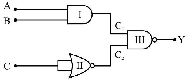
72. The logic circuit shown in the circuit below yeilds the truth table as given below. The gate ’

(1) OR gate
(2) AND gate
(3) NAND gate
(4) NOR gate
Show Answer
Correct answer: (2)
Solution:
From the above circuit
i.e. it is for OR gate:
or
| 0 | 1 | 0 | 0 | 0 |
| 0 | 1 | 1 | 0 or 1 | 1 |
| 1 | 0 | 0 | 0 or 1 | 1 |
| 1 | 0 | 1 | 0 or 1 | 1 |
Let
| 0 | 1 | 0 | 0 | 0 |
| 0 | 1 | 1 | 1 | 1 |
| 1 | 0 | 0 | 0 or 1 | 1 |
| 1 | 0 | 1 | 0 or 1 | 1 |
For gate
| 0 | 0 | 0 |
| 0 | 1 | 0 |
| 1 | 0 | 0 |
| 1 | 1 | 1 |
This is truth table of AND gate. Therefore
Average
Logic Gate
73. For the circutal arrangement shown the TRUTH table is

(1)
| 0 | 0 | 1 |
| 1 | 0 | 1 |
| 0 | 1 | 1 |
| 1 | 1 | 1 |
(2)
| 0 | 0 | 0 |
| 1 | 0 | 0 |
| 0 | 1 | 1 |
| 1 | 1 | 1 |
(3)
| 0 | 0 | 1 |
| 1 | 0 | 1 |
| 0 | 1 | 0 |
| 1 | 1 | 0 |
(4)
| 0 | 0 | 1 |
| 1 | 0 | 1 |
| 0 | 1 | 1 |
| 1 | 1 | 0 |
Show Answer
Correct answer: (4)
Solution:
Gate I and II are NOR gates with the two inputs joined together. Each gate acts as a NOT gate. The inputs of gate III are
| 0 | 0 | 1 | 1 | 1 |
| 0 | 1 | 1 | 0 | 1 |
| 1 | 0 | 0 | 1 | 1 |
| 1 | 1 | 0 | 0 | 0 |
Average
Logic Gates
74. The signals A and B shown in Fig. (a) are the used as inputs in circuit shown in FIg. (b). The output signal

(1)

(2)

(3)

(4)

Show Answer
Correct answer: (1)
Solution:
Gate
| 1 | 0 | 0 | 1 |
| 0 | 1 | 1 | 0 |
| 0 | 1 | 1 | 0 |
| 1 | 0 | 0 | 1 |
| 1 | 1 | 0 | 1 |
| 0 | 1 | 1 | 0 |
The pluse representation of

Difficult
Logic Gates
75. The Booliean representation of a logic cate circuit using two inputs
The correct circuit is:
(1)
(2)
(3)
(4)
Show Answer
Correct answer: (3)
Solution:
Let
Difficult
Logic Gates
76. Four NAND gates are connected as shown in Fig. The arrangment is equivalent to
(1) One NAND gate
(2) One OR gate
(3) One NOR gate
(4) One NOT gate
Show Answer
Correct answer: (1)
Solution:
Gate I and II are used as NAND gates. Let their output be
| 0 | 0 | 1 | 1 | 0 | 1 |
| 0 | 1 | 1 | 1 | 0 | 1 |
| 1 | 0 | 1 | 1 | 0 | 1 |
| 1 | 1 | 0 | 0 | 1 | 0 |
From the truth-table we can make truth-table showing A, B and C only. This is truth-table of a NAND gate. The arrangment therefore is equivalent to a single NAND gate.
Average
Logic Gates
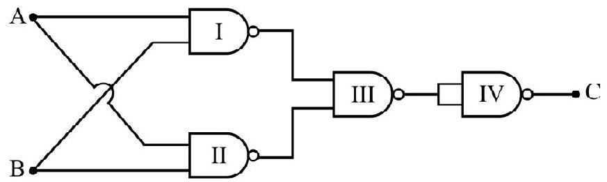
77. In the circuit shown in Fig. the output
(1)
(2)
(3)
(4)
Show Answer
Correct answer: (4)
Solution:
Gate I is AND gate; gate II is NOR gate used as a NOT gate and gate III is NAND gate.
The correct choice is (4).
Difficult
Logic Gates
78. Fig. shows a logic commbination with
(1)
(2)
(3)
(4)
Show Answer
Correct answer: (3)
Solution:
Difficult
Logic Gates
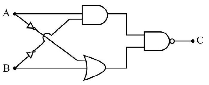
79. Four NAND gates are joined together as shown in Fig; then the correct Truth-table of the arrangement is
(1)
| 0 | 0 | 0 |
| 0 | 1 | 1 |
| 1 | 0 | 1 |
| 1 | 1 | 0 |
(2)
| 0 | 0 | 0 |
| 0 | 1 | 0 |
| 1 | 0 | 1 |
| 1 | 1 | 1 |
(3)
| 0 | 0 | 1 |
| 0 | 1 | 1 |
| 1 | 0 | 0 |
| 1 | 1 | 0 |
(4)
| 0 | 0 | 1 |
| 0 | 1 | 0 |
| 1 | 0 | 0 |
| 1 | 1 | 1 |
Show Answer
Correct answer: (1)
Solution:
Difficult
Logic Gate
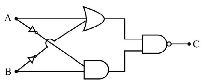
80. For the arrangment of logic gates shown in Fig. the Truth-table is
(1)
| 0 | 0 | 0 |
| 0 | 1 | 1 |
| 1 | 0 | 1 |
| 1 | 1 | 1 |
(2)
| 0 | 0 | 1 |
| 0 | 1 | 0 |
| 1 | 0 | 0 |
| 1 | 1 | 1 |
(3)
| 0 | 0 | 1 |
| 0 | 1 | 1 |
| 1 | 0 | 0 |
| 1 | 1 | 0 |
(4)
| 0 | 0 | 1 |
| 0 | 1 | 1 |
| 1 | 0 | 1 |
| 1 | 1 | 1 |
Show Answer
Correct answer: (4)
Solution:
Gate I, II and III are NOR gates and gate IV is NAND gate. Using the truth tables of gate involved we have
| 0 | 0 | 1 | 0 | 0 | 1 |
| 0 | 1 | 0 | 1 | 0 | 1 |
| 1 | 0 | 0 | 0 | 1 | 1 |
| 1 | 1 | 0 | 0 | 0 | 1 |
In Fig. the gates have been numbered as I, II, III and IV. Their outputs are labled as
| 0 | 0 | 1 | 1 | 1 | 0 |
| 0 | 1 | 1 | 1 | 0 | 1 |
| 1 | 0 | 1 | 0 | 1 | 1 |
| 1 | 1 | 0 | 1 | 1 | 0 |
In terms A, B and Y the correct Truth-table is given in (1).