Chapter 14 Semiconductor Electronics Material Devices and Simple Circuit
Multiple Choice Questions (MCQs)
1. The conductivity of a semiconductor increases with increase in temperature, because
(a) number density of free current carries increases
(b) relaxation time increases
(c) both number density of carries and relaxation time increase
(d) number density of carries increases, relaxation time decreases but effect of decrease in relaxation time is much less than increase in number density
Show Answer
Answer
(d) The conductivity of a semiconductor increases with increase in temperature, because the number density of current carries increases, relaxation time decreases but effect of decrease in relaxation is much less than increase in number density.
2. In figure given below $V_0$ is the potential barrier across a $p-n$ junction, when no battery is connected across the junction
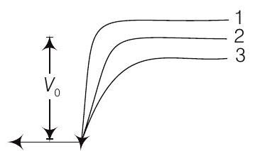
(a) 1 and 3 both correspond to forward bias of junction
(b) 3 corresponds to forward bias of junction and 1 corresponds to reverse bias of junction
(c) 1 corresponds to forward bias and 3 corresponds to reverse bias of junction
(d) 3 and 1 both correspond to reverse bias of junction
Show Answer
Thinking Process
Go through the working of p-njunction.
Answer
(b) When $p-n$ junction is forward biased, it opposes the potential barrier junction, when $p-n$ junction is reverse biased, it supports the potential barrier junction, resulting increase in potential barrier across the junction.
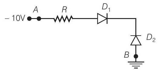
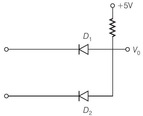
3. In figure given below, assuming the diodes to be ideal
(a) $D_1$ is forward biased and $D_2$ is reverse biased and hence current flows from $A$ to $B$
(b) $D_2$ is forward biased and $D_1$ is reverse biased and hence no current flows from $B$ to $A$ and vice-versa
(c) $D_1$ and $D_2$ are both forward biased and hence current flows from $A$ to $B$
(d) $D_1$ and $D_2$ are both reverse biased and hence no current flows from $A$ to $B$ and vice-versa
Show Answer
Thinking Process
Check the polarity of the diodes.
Answer
(b) In the given circuit $p$-side of $p$ - $n$ function $D_1$ is connected to lower voltage and $n$-side of $D_1$ to higher voltage.
Thus $D$ is reverse biased.
The $p$-side of $p$ - $n$ junction $D_2$ is at higher potential and $n$-side of $D_2$ is at lower potential. Therefore $D_2$ is forward biased.
Hence, current flows through the junction $B$ to $A$.
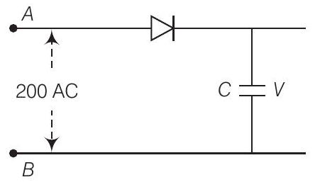
4. A $220 V$ AC supply is connected between points $A$ and $B$ (figure). What will be the potential difference $V$ across the capacitor?
 $\newline$
(a) $220 V$ $\newline$
(b) $110 V$ $\newline$
(c) $0 V$ $\newline$
(d) $220 \sqrt{2} V$ $\newline$
Show Answer
Thinking Process
$p$-n junction conducts during positive half cycle only.
Answer
(d) As $p$ - $n$ junction conducts during positive half cycle only, the diode connected here will work is positive half cycle. Potential difference across $C=$ peak voltage of the given $A C$ voltage $=V_0=V_{\text {rms }} \sqrt{2}=220 \sqrt{2} V$.
5. Hole is
(a) an anti-particle of electron
(b) a vacancy created when an electron leaves a covalent bond
(c) absence of free electrons
(d) an artificially created particle
Show Answer
Answer
(b) The concept of hole describes the lack of an electron at a position where one could exist in an atom or atomic lattice. If an electron is excited into a higher state, it leaves a hole in its old state.
Thus, hole can be defined as a vacancy created when an electron leaves a covalent bond.
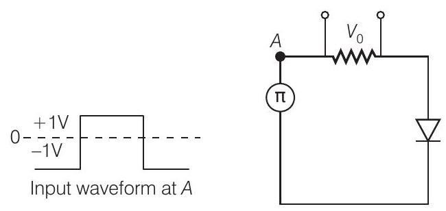
6. The output of the given circuit in figure given below,
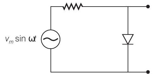
(a) would be zero at all times
(b) would be like a half wave rectifier with positive cycles in output
(c) would be like a half wave rectifier with negative cycles in output
(d) would be like that of a full wave rectifier
Show Answer
Thinking Process
For positive half cycle of input AC voltage, the p-n junction is forward biased and for negative half cycle of input $A C$ voltage the $p$ - $n$ junction is reversed biased.
Answer
(c) Due to forward biased during positive half cycle of input AC voltage, the resistance of $p-n$ junction is low. The current in the circuit is maximum. In this situation, a maximum potential difference will appear across resistance connected in series of circuit. This result into zero output voltage across $p-n$ junction.
Due to reverse biase during negative half cycle of $A C$ voltage, the $p-n$ junction is reverse biased. The resistance of $p-n$ junction becomes high which will be more than resistance in series. That is why, there will be voltage across $p-n$ junction with negative cycle in output.
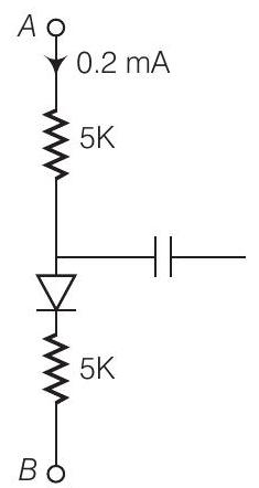
7. In the circuit shown in figure given below, if the diode forward voltage drop is $0.3 V$, the voltage difference between $A$ and $B$ is
(a)
 $\newline$
(a) $1.3 V$ $\newline$
(b) $2.3 V$ $\newline$
(c) 0 $\newline$
(d) $0.5 V$ $\newline$
MTMM
Show Answer
Answer
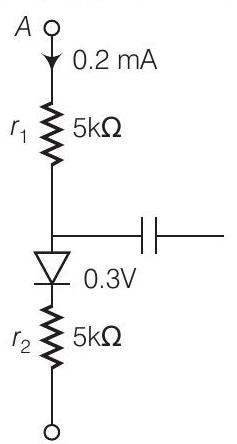
(b) Consider the fig. (b) given here, suppose the potential difference between $A$ and $B$. $r_1=5 k \Omega$ and $r_2=5 k \Omega$ are resistance in series connection.
$$ \begin{matrix} \text { Then, } \quad V-0.3 & .=[(r_1+r_2) 10^{3}] \times(0.2 \times 10^{-3})] & {[\because V=i r]} \\ & =[(5+5) 10^{3}] \times(0.2 \times 10^{-3}) & \\ & =10 \times 10^{3} \times 0.2 \times 10^{-3}=2 & \\ \Rightarrow \quad V & =2+0.3=2.3 V \end{matrix} $$
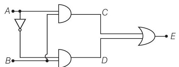
8. Truth table for the given circuit is
(a)
| $A$ | $B$ | $E$ |
|---|---|---|
| 0 | 0 | 1 |
| 0 | 1 | 0 |
| 1 | 0 | 1 |
| 1 | 1 | 0 |
(b)
| $A$ | $B$ | $E$ |
|---|---|---|
| 0 | 0 | 1 |
| 0 | 1 | 0 |
| 1 | 0 | 0 |
| 1 | 1 | 0 |
(c)
| $A$ | $B$ | $E$ |
|---|---|---|
| 0 | 0 | 0 |
| 0 | 1 | 1 |
| 1 | 0 | 0 |
| 1 | 1 | 1 |
(d)
| $A$ | $B$ | $E$ |
|---|---|---|
| 0 | 0 | 0 |
| 0 | 1 | 1 |
| 1 | 0 | 1 |
| 1 | 1 | 0 |
Show Answer
Answer
(c) Here,
$$ \begin{aligned} C & =A \cdot B \text { and } D=\bar{A} \cdot B \\ E & =C+D=(A \cdot B)+(\bar{A} \cdot B) \end{aligned} $$
Explanation The truth table of this arrangement of gates can be given by
| $\boldsymbol{A}$ | $\boldsymbol{B}$ | $\overline{\boldsymbol{A}}$ | $\boldsymbol{C}=\boldsymbol{A} \cdot \boldsymbol{B}$ | $\boldsymbol{d}=\overline{\boldsymbol{A}} \cdot \boldsymbol{B}$ | $\boldsymbol{E}=(\boldsymbol{C}+\boldsymbol{D})$ |
|---|---|---|---|---|---|
| 0 | 0 | 1 | 0 | 0 | 0 |
| 0 | 1 | 1 | 0 | 1 | 1 |
| 1 | 0 | 0 | 0 | 0 | 0 |
| 1 | 1 | 0 | 1 | 0 | 1 |
$\newline$
Multiple Choice Questions (More Than One Options)
9. When an electric field is applied across a semiconductor
(a) electrons move from lower energy level to higher energy level in the conduction band
(b) electrons move from higher energy level to lower energy level in the conduction band
(c) holes in the valence band move from higher energy level to lower energy level
(d) holes in the valence band move from lower energy level to higher energy level
Show Answer
Thinking Process
Electrons are negatively charged and its energy increases when electric fields is applied.
Answer
(a, c)
When electric field is applied across a semiconductor, the electrons in the conduction band get accelerated and acquire energy. They move from lower energy level to higher energy level. While the holes in valence band move from higher energy level to lower energy level, where they will be having more energy.
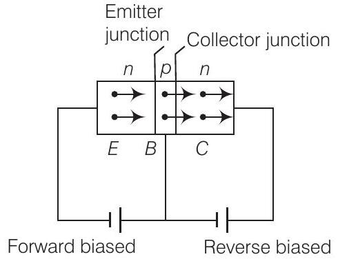
10. Consider an $n-p-n$ transitor with its base-emitter junction forward biased and collector base junction reverse biased. Which of the following statements are true?
(a) Electrons crossover from emitter to collector
(b) Holes move from base to collector
(c) Electrons move from emitter to base
(d) Electrons from emitter move out of base without going to the collector.
Show Answer
Thinking Process
Draw the figure as given in the question.
Answer
$(a, c)$
Here emitter-base junction is forward biased i.e., the positive pole of emitter base battery is connected to base and its negative pole to emitter. Also, the collector base junction is reverse biased, i.e., the positive pole of the collector base battery is connected to collector and negative pole to base.
Thus, electron move from emmiter to base and crossover from emitter to collector.
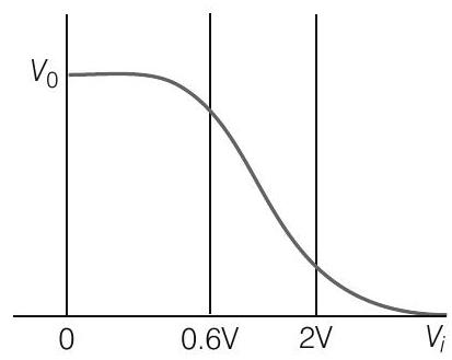
11. Figure given below shows that transfer characteristics of a base biased CE transistor. Which of the following statements are true?
(a) At $V_{i}=0.4 V$, transistor is in active state
(b) At $V_{i}=1 V$, it can be used as an amplifier
(c) At $V_{i}=0.5 V$, it can be used as a switch turned off
(d) At $V_{i}=2.5 V$, can be used as a switch turned on
Show Answer
Answer
$(b, c, d)$
From the given transfer characteristics of a base biased common emitter transistor, we note that
(i) when $V_{i}=0.4 V$, there is no collection current. The transistor circuit is in active state and is used as an amplifier.
(ii) when $V_{i}=1 V$ (This is in between $0.6 V$ to $2 V$ ), the transistor circuit is in active state and is used as an amplifier.
(iii) when $V_{i}=0.5 V$, there is no collector current. The transistor is in cut off state. The transistor circuit can be used as a switch turned off.
(iv) when $V_{i}=2.5 V$, the collector current becomes maximum and transistor is in saturation state and can used as switch turned on state.
12. In a $n-p-n$ transistor circuit, the collector current is $10 mA$. If 95 per cent of the electrons emitted reach the collector, which of the following statements are true?
(a) The emitter current will be $8 mA$
(b) The emitter current will be $10.53 mA$
(c) The base current will be $0.53 mA$
(d) The base current will be $2 mA$
Show Answer
Thinking Process
The collector current is the $95 %$ of electrons reaching the collector after emission.
Answer
$(b, c)$
Here,
Also
$\Rightarrow \quad I_{e}=\frac{10 \times 100}{95}=10.53 mA$
Also,
$$ \begin{aligned} & I_{C}=10 mA \\ & I_{c}=\frac{95}{100} I_{e} \\ & I_{e}=\frac{10 \times 100}{95}=10.53 mA \\ & I_{b}=I_{e}-I_{C}=10.53-10=0.53 mA \end{aligned} $$
13. In the depletion region of a diode
(a) there are no mobile charges
(b) equal number of holes and elections exist, making the region neutral
(c) recombination of holes and electrons has taken place
(d) immobile charged ions exist
Show Answer
Answer
$(a, b, d)$
The space-charge regions on both the sides of $p-n$ junction which has immobile ions and entirely lacking of any charge carriers will form a region called depletion region of a diode. The number of ionized acceptors on the $p$-side equals the number of ionized donors on the $n$-side.
14. What happens during regulation action of a Zener diode?
(a) The current and voltage across the Zener remains fixed
(b) The current through the series Resistance $(R_{s})$ changes
(c) The Zener resistance is constant
(d) The resistance offered by the Zener changes
Show Answer
Answer
$(b, d)$
During regulation action of a Zener diode, the current through the $R_{s}$ changes and resistance offered by the Zener changes. The current through the Zener changes but the voltage across the Zener remains constant.
15. To reduce the ripples in rectifier circuit with capacitor filter
(a) $R_{L}$ should be increased
(b) input frequency should be decreased
(c) input frequency should be increased
(d) capacitors with high capacitance should be used
Show Answer
Thinking Process
Ripple factor ( $r$ ) of a full wave rectifier using capacitor filter is given by
$$ \begin{matrix} r & =\frac{1}{4 \sqrt{3} R_{L} C_{V}} \\ \text { i.e., } \quad r \propto \frac{1}{R_{L}} \Rightarrow r \propto \frac{1}{C}, r \propto \frac{1}{V} \end{matrix} $$
Answer
$(a, c, d)$
Ripple factor is inversely proportional to $R_{L}, C$ and $v$.
Thus to reduce $r, R_{L}$ should be increased, input frequency $v$ should be increased and capacitance $C$ should be increased.
16. The breakdown in a reverse biased $p-n$ junction is more likely to occur due to
(a) large velocity of the minority charge carriers if the doping concentration is small
(b) large velocity of the minority charge carriers if the doping concentration is large
(c) strong electric field in a depletion region if the doping concentration is small
(d) strong electric field in the depletion region if the doping concentration is large
Show Answer
Answer
$(a, d)$
In reverse biasing, the minority charge carriers will be accelerated due to reverse biasing, which on striking with atoms cause ionization resulting secondary electrons and thus more number of charge carriers.
When doping concentration is large, there will be large number of ions in the depletion region, which will give rise to a strong electric field.
Very Short Answer Type Questions
17. Why are elemental dopants for Silicon or Germanium usually chosen from group XIII or group XV?
Show Answer
Answer
The size of the dopant atom should be such that their presence in the pure semiconductor does not distort the semiconductor but easily contribute the charge carriers on forming covalent bonds with $Si$ or $Ge$ atoms, which are provided by group XIII or group XV elements.
18. $ \text {Sn, C and i, Ge are all group XIV elements. }$ Yet, Sn is a conductor, C is an insulator while Si and Ge are semiconductors. Why?
Show Answer
Thinking Process
The property of conduction level of any element depends on the energy gap between its conduction band and valence band.
Answer
A material is a conductor if in its energy band diagram, there is no energy gap between conduction band and valence band. For insulator, the energy gap is large and for semiconductor the energy gap is moderate.
The energy gap for $Sn$ is $0 eV$, for $C$ is $5.4 eV$, for $Si$ is $1.1 eV$ and for $Ge$ is $0.7 eV$, related to their atomic size. Therefore $Sn$ is a conductor, $C$ is an insulator and $Ge$ and $Si$ are semiconductors.
19. Can the potential barrier across a $p-n$ junction be measured by simply connecting a voltmeter across the junction?
Show Answer
Answer
We cannot measure the potential barrier across a $p-n$ junction by a voltmeter because the resistance of voltmeter is very high as compared to the junction resistance.
20. Draw the output waveform across the resistor in the given figure.
Show Answer
Answer
As we know that the diode only works in forward biased, so the output is obtained only when positive input is given, so the output waveform is
21. The amplifiers $X, Y$ and $Z$ are connected in series. If the voltage gains of $X, Y$ and $Z$ are 10, 20 and 30 , respectively and the input signal is $1 mV$ peak value, then what is the output signal voltage (peak value) (i) if DC supply voltage is $10 V$ ? (ii) if DC supply voltage is $5 V$ ?
Show Answer
Thinking Process
$\frac{\text { Output signal voltage }}{\text { Input Signal voltage }}=$ Total voltage amplification
Answer
Given,
$$ A v_{x}=10, A v_{y}=20, A v_{z}=30 $$
$$ \Delta V_{i}=1 mV=10^{-3} V $$
Now, $\quad \frac{\text { Output Signal Voltage }(\Delta V_0)}{\text { Input Singal Voltage }(\Delta V_{i})}=$ Total voltage amplification
$$ =A v_{x} \times A v_{y} \times A v_{z} $$
$\Rightarrow$
$$ \begin{aligned} \Delta V_0 & =A v_{x} \times A v_{y} \times A v_{z} \times \Delta V_{i} \\ & =10 \times 20 \times 30 \times 10^{-3}=6 V \end{aligned} $$
(i) If DC supply voltage is $10 V$, then output is $6 V$, since theoretical gain is equal to practical gain, i.e., output can never be greater than $6 V$.
(ii) If $DC$ supply voltage is $5 V$, i.e., $V_{c c}=5 V$. Then, output peak will not exceed $5 V$. Hence $V_0=5 V$.
22. In a CE transistor amplifier, there is a current and voltage gain associated with the circuit. In other words there is a power gain. Considering power a measure of energy, does the circuit violate conservation of energy?
Show Answer
Answer
In CE transistor amplifier, the power gain is very high.
In this circuit, the extra power required for amplified output is obtained from DC source. Thus, the circuit used does not violet the law of conservation.
Short Answer Type Questions
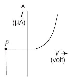
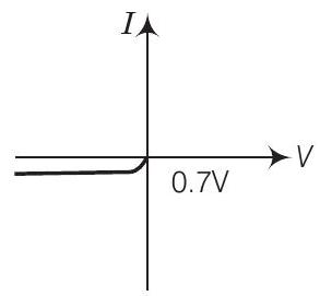
23. (i) Name the type of a diode whose characteristics are shown in figure. (a) and (b).
(ii) What does the point $P$ in fig. (a) represent?
(iii) What does the points $P$ and $Q$ in fig. (b) represent?
(a)
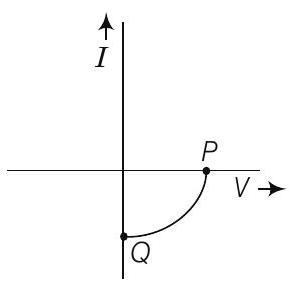
(b)
Show Answer
Answer
(i) The characteristic curve (a) is of Zener diode and curve (b) is of solar cell.
(ii) The point $P$ in fig. (a) represents Zener break down voltage.
(iii) In fig. (b), the point $Q$ represents zero voltage and negative current. It means light falling on solar cell with atleast minimum threshold frequency gives the current in opposite direction to that due to a battery connected to solar cell. But for the point $Q$, the battery is short circuited. Hence represents the short circuit current.
In fig. (b), the point $P$ represents some positive voltage on solar cell with zero current through solar cell.
It means, there is a battery connected to a solar cell which gives rise to the equal and opposite current to that in solar cell by virtue of light falling on it.
As current is zero for point $P$, hence we say $P$ represents open circuit voltage.
24. Three photo diodes $D_1, D_2$ and $D_3$ are made of semiconductors having band gaps of $2.5 eV, 2 eV$ and $3 eV$, respectively. Which ones will be able to detect light of wavelength $6000 \AA$ ?
Show Answer
Answer
Given, wavelength of light $\lambda=6000 \AA=6000 \times 10^{-10} m$
Energy of the light photon
$$ E=\frac{h c}{\lambda}=\frac{6.6 \times 10^{-34} \times 3 \times 10^{8}}{6000 \times 10^{-10} \times 1.6 \times 10^{-19}} eV=2.06 eV $$
The incident radiation which is detected by the photodiode having energy should be greater than the band-gap. So, it is only valid for diode $D_2$. Then, diode $D_2$ will detect this radiation.
25. If the resistance $R_1$ is increased (see figure), how will the readings of the ammeter and voltmeter change?
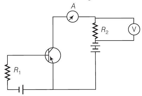
Show Answer
Answer
Consider the circuit in fig. (b) to find the change in reading As we know the formula for base current, $I_{B}=\frac{V_{BB}-V_{BE}}{R_{i}}$
As $R_{i}$ is increased, $I_{B}$ is decreased.
Now, the current in ammeter is collector current $I_{C}$.
$I_{C}=\beta I_{B}$ as $I_{B}$ decreased $I_{C}$ also decreased and the reading of voltmeter and ammeter also decreased.
26. Two car garages have a common gate which needs to open automatically when a car enters either of the garages or cars enter both. Devise a circuit that resembles this situation using diodes for this situation.
Show Answer
Answer
As car enters in the gate, any one or both are opened.
The device is shown.
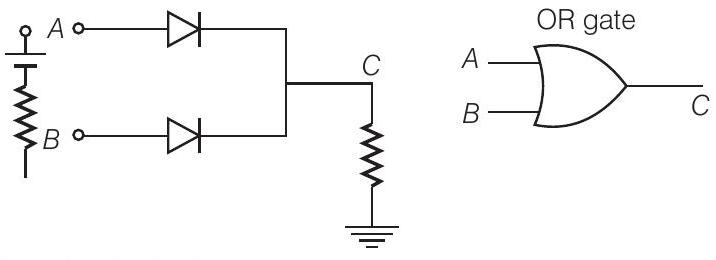
So, OR gate gives the desired output.
| $\boldsymbol{A}$ | $\boldsymbol{B}$ | $\boldsymbol{C}$ |
|---|---|---|
| 0 | 0 | 0 |
| 0 | 1 | 1 |
| 1 | 0 | 1 |
| 1 | 1 | 1 |
27. How would you set up a circuit to obtain NOT gate using a transistor?
Show Answer
Answer
The NOT gate is a device which has only one input and one output i.e., $\bar{A}=Y$ means $Y$ equals NOT $A$.
This gate cannot be realised by using diodes. However it can be realised by making use of a transistor. This can be seen in the figure given below
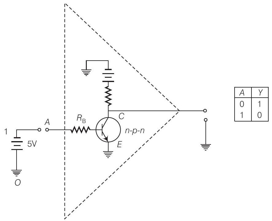
Here, the base $B$ of the transistor is connected to the input $A$ through a resistance $R_{b}$ and the emitter $E$ is earthed. The collector is connected to $5 V$ battery. The output $Y$ is the voltage at $C$ w.r.t. earth.
The resistor $R_{b}$ and $R_{c}$ are so chosen that if emitter-base junction is unbiased, the transistor is in cut off mode and if emitter-base junction is forward biased by $5 V$, the transistor is in saturation state.
28. Explain why elemental semiconductor cannot be used to make visible LEDs.
Show Answer
Answer
In elemental semiconductor, the band gap is such that the emission are in infrared region and not in visible region.
29. Write the truth table for the circuit shown in figure given below. Name the gate that the circuit resembles.
Show Answer
Answer
The circuit resemble AND gate. The boolean expression of this circuit is, $V_0=A$.Bi.e., $V_0$ equals A AND B. The truth table of this gate is as given below
| A | B | $V_0 = A$ |
|---|---|---|
| 0 | 0 | 0 |
| 0 | 1 | 0 |
| 1 | 0 | 0 |
| 1 | 1 | 1 |
30. A Zener of power rating $1 W$ is to be used as a voltage regulator. If Zener has a breakdown of $5 V$ and it has to regulate voltage which fluctuated between $3 V$ and $7 V$, what should be the value of $R_{s}$ for safe operation (see figure)?
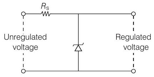
Show Answer
Answer
Given,
$$ \begin{aligned} \text { power } & =1 W \\ \text { Zener breakdown } V_{z} & =5 V \\ \text { Minimum voltage } V_{\min } & =3 V \\ \text { Maximum voltage } V_{\max } & =7 V \\ \text { Current } I_{Z_{\max }} & =\frac{P}{V_{Z}}=\frac{1}{5}=0.2 A \end{aligned} $$
The value of $R_{s}$ for safe operation $R_{s}=\frac{V_{\max }-V_{Z}}{I_{Z_{\max }}}=\frac{7-5}{0.2}=\frac{2}{0.2}=10 \Omega$
Long Answer Type Questions
31. If each diode in figure has a forward bias resistance of $25 \Omega$ and infinite resistance in reverse bias, what will be the values of the currents $I_1, I_2, I_3$ and $I_4$ ?
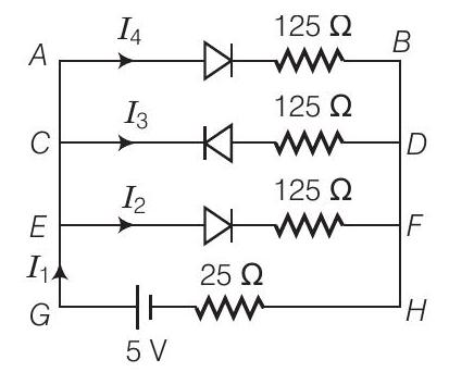
Show Answer
Answer
Given, forward biased resistance $=25 \Omega$
Reverse biased resistance $=\infty$
As the diode in branch $C D$ is in reverse biased which having resistance infinite,
$$ \text{So}\qquad I_3=0 $$
Resistance in branch $A B=25+125=150 \Omega$ say $R_1$
Resistance in branch $E F=25+125=150 \Omega$ say $R_2$
$A B$ is parallel to $E F$.
So, $\quad$ resultant resistance $\frac{1}{R^{\prime}}=\frac{1}{R_1}+\frac{1}{R_2}=\frac{1}{150}+\frac{1}{150}=\frac{2}{150}$
$$ \Rightarrow \qquad R^{\prime}=75 \Omega $$
Total resistance $R=R^{\prime}+25=75+25=100 \Omega$
$$ \text{Current}\hspace{1mm}I_1=\frac{V}{R}=\frac{5}{100}=0.05 A$$
$$ \begin{aligned} & I_1=I_4+I_2+I_3 \qquad \text { (Here } I_3=0 \text { ) } \\ So,\qquad & I_1=I_4+I_2 \end{aligned} $$
Here,the resistances $R_1$ and $R_2$ is same.
$$ i.e.,\qquad I_4=I_2 $$
$$ \begin{matrix} \therefore & I_1=2 I_2 \\ \Rightarrow \qquad & I_2=\frac{I_1}{2}=\frac{0.05}{2}=0.025 A \end{matrix} $$
$$ \text{and}\qquad I_4=0.025 A $$
Thus, $\quad I_1=0.05 A, I_2=0.025 A, I_3=0$ and $I_4=0.025 A$
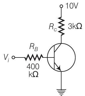
32. In the circuit shown in figure, when the input voltage of the base resistance is $10 V, V_{BE}$ is zero and $V_{CE}$ is also zero. Find the values of $I_{B}, I_{C}$ and $\beta$.
Show Answer
Answer
Given,
$$ \begin{aligned} \text { voltage across } R_{B} & =10 V \\ \text { Resistance } R_{B} & =400 k \Omega \\ V_{BE} & =0, V_{CE}=0 R_{C}=3 k \Omega \\ I_{B} & =\frac{\text { Voltage across } R_{B}}{R_{B}} \\ & =\frac{10}{400 \times 10^{3}}=25 \times 10^{-6} A=25 \mu A \end{aligned} $$
Voltage across $R_{C}=10 V$
$$ \begin{aligned} I_{C} & =\frac{\text { Voltage across } R_{C}}{R_{C}}=\frac{10}{3 \times 10^{3}} \\ & =3.33 \times 10^{-3} A=3.33 mA \\ \beta & =\frac{I_{C}}{I_{B}}=\frac{3.33 \times 10^{-3}}{25 \times 10^{-6}} \\ & =1.33 \times 10^{2}=133 \end{aligned} $$
Semiconductor Electronics : Material, Devices and Simple Circuit 241
33. Draw the output signals $C_1$ and $C_2$ in the given combination of gates.

Show Answer
Answer
First draw the truth table of $C_1$ and $C_2$.
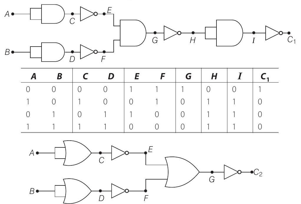
| A | $\boldsymbol{B}$ | $\boldsymbol{C}$ | $\boldsymbol{D}$ | $\boldsymbol{E}$ | $\boldsymbol{F}$ | $\boldsymbol{G}$ | $C_2$ |
|---|---|---|---|---|---|---|---|
| 0 | 0 | 0 | 0 | 1 | 1 | 1 | 0 |
| 1 | 0 | 1 | 0 | 0 | 1 | 1 | 0 |
| 0 | 1 | 0 | 1 | 1 | 0 | 1 | 0 |
| 1 | 1 | 1 | 1 | 0 | 0 | 0 | 1 |
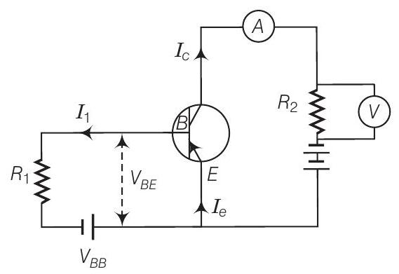
34. Consider the circuit arrangement shown in figure for studying input and output characteristics of $n-p-n$ transistor in CE configuration.
Select the values of $R_{B}$ and $R_{C}$ for a transistor whose $V_{BE}=0.7 V$, so that the transistor is operating at point $Q$ as shown in the characteristics (see figure).
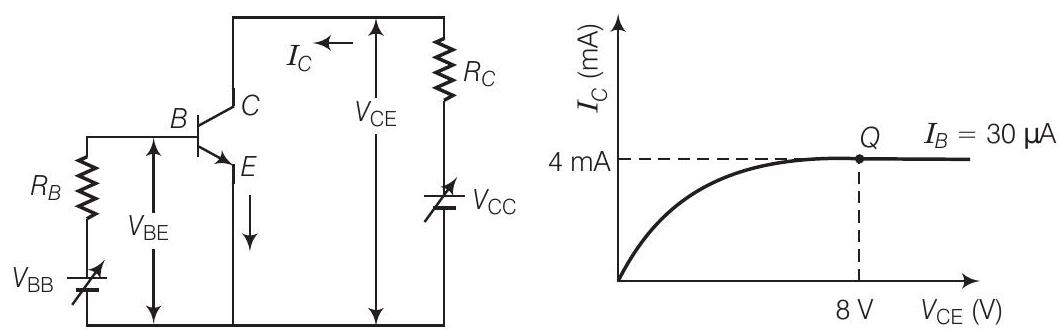
Given that the input impedance of the transistor is very small and $V_{C C}=V_{B B}=16 V$, also find the voltage gain and power gain of circuit making appropriate assumptions.
Show Answer
Answer
Given,
$$ \begin{aligned} V_{B E} & =0.7 V, V_{C C}=V_{B B}=16 V \\ V_{C E} & =8 V \qquad \text{(from graph)} \\ I_{C} & =4 mA=4 \times 10^{-3} A \\ I_{B} & =30 \mu A=30 \times 10^{-6} A \end{aligned} $$
For the output characteristic at $\theta$
$$ \begin{aligned} & V_{C C}=I_{C} R_{C}+V_{C E} \\ & R_{C}=\frac{V_{C C}-V_{C E}}{I_{C}}=\frac{16-8}{4 \times 10^{-3}}=\frac{8 \times 1000}{4}=2 k \Omega \end{aligned} $$
Using the relation,
$$ V_{BB}=I_{B} R_{B}+V_{BE} $$
$$ \begin{aligned} R_{B} & =\frac{V_{BB}-V_{BE}}{I_{B}}=\frac{16-0.7}{30 \times 10^{-6}} \\ & =510 \times 10^{3} \Omega=510 k \Omega \\ \beta & =\frac{I_{C}}{I_{B}}=\frac{4 \times 10^{-3}}{30 \times 10^{-6}}=133 \end{aligned} $$
Voltage gain $=\beta \frac{R_{C}}{R_{B}}=\frac{133 \times 2 \times 10^{3}}{510 \times 10^{3}}=0.52$
Power gain $=\beta \times$ Voltage gain $=133 \times 0.52=69$
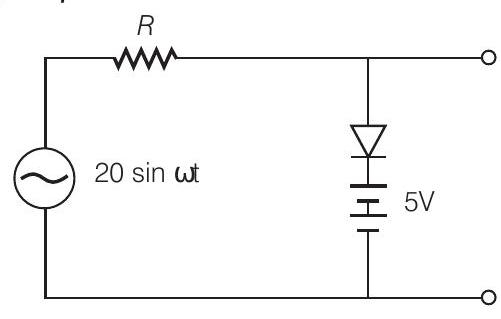
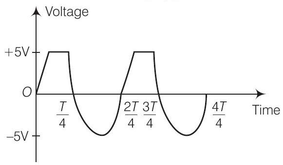
35. Assuming the ideal diode, draw the output waveform for the circuit given in fig. (a), explain the waveform.
Show Answer
Thinking Process
An ideal diode is a diode that acts like a perfect conductor when voltage is applied forward biased and like a perfect insulator when voltage is applied reverse biased.
Answer
When the input voltage is equal to or less than $5 V$, diode will be revers biased. It will offer high resistance in comparison to resistance $(R)$ in series. Now, diode appears in open circuit. The input waveform is then passed to the output terminals. The result with sin wave input is to dip off all positive going portion above $5 V$.
If input voltage is more than $+5 V$, diode will be conducting as if forward biased offering low resistance in comparison to $R$. But there will be no voltage in output beyond $5 V$ as the voltage beyond $+5 \vee$ will appear across $R$.
When input voltage is negative, there will be opposition to $5 V$ battery in $p-n$ junction input voltage becomes more than $-5 V$, the diode will be reverse biased. It will offer high resistance in comparison to resistance $R$ in series. Now junction diode appears in open circuit. The input wave form is then passed on to the output terminals.
The output waveform is shown here in the fig. (b)
36. Suppose a $n$-type wafer is created by doping $Si$ crystal having $5 \times 10^{28}$ atoms $/ m^{3}$ with $\text{1 ppm}$ concentration of As. On the surface $200 \text{ppm}$ boron is added to create ’ $p$ ’ region in this wafer. Considering $n_{i}=1.5 \times 10^{16} m^{-3}$, (i) Calculate the densities of the charge carriers in the $n$ and $p$ regions. (ii) Comment which charge carriers would contribute largely for the reverse saturation current when diode is reverse biased.
Show Answer
Answer
When As is implanted in Si crystal, $n$ - type wafer is created. The number of majority carriers electrons due to doping of As is
$$ \begin{aligned} n_{e} & =N_{D}=\frac{1}{10^{6}} \times 5 \times 10^{28} \\ & =5 \times 10^{22} / m^{3} \end{aligned} $$
Number of minority carriers (holes) in $n$-type wafer is
$$ \begin{aligned} n_{h} & =\frac{n_i^{2}}{n_{e}}=\frac{(1.5 \times 10^{16})^{2}}{5 \times 10^{22}} \\ & =0.45 \times 10^{10} / m^{3} \end{aligned} $$
When $B$ is implanted in Si crystal, $p$-type wafer is created with number of holes,
$$ n_{h}=N_{A}=\frac{200}{10^{6}} \times(5 \times 10^{28})=1 \times 10^{25} / m^{3} $$
Minority carriers (electrons) created in $p$ - type wafer is
$$ \begin{aligned} n_{e} & =\frac{n_i^{2}}{n_{h}}=\frac{(1.5 \times 10^{16})^{2}}{1 \times 10^{25}} \\ & =2.25 \times 10^{27} / m^{3} \end{aligned} $$
When $p-n$ junction is reverse biased, the minority carrier holes of $n$-region wafer $(n_{h}=0.45 \times 10^{10} / m^{3})$ would contribute more to the reverse saturation current than minority carrier electrons $(n_{e}=2.25 \times 10^{7} / m^{3})$ of pregion wafer.
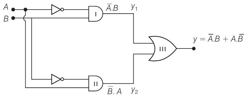
37. An X-OR gate has following truth table.
| A | B | Y |
|---|---|---|
| 0 | 0 | 0 |
| 0 | 1 | 1 |
| 1 | 0 | 1 |
| 1 | 1 | 0 |
It is represented by following logic relation $Y=\bar{A} \cdot B+A \cdot \bar{B}$
Build this gate using AND, OR and NOT gates.
Show Answer
Answer
Given, the logic relation for the given truth table is
$$ \begin{aligned} Y & =\bar{A} \cdot B+A \cdot \bar{B}=Y_1+Y_2 \\ Y_1 & =A \cdot B \text { and } Y_2=A \cdot \bar{B} \end{aligned} $$
$Y_1$ can be obtained as output of AND gate I for which one Input is of $A$ through NOT gate and another input is of $B$. $Y_2$ can be obtained as output of AND gate II for which one input is of $A$ and other input is of $B$ through NOT gate.
Now $Y_2$ can be obtained as output from OR gate, where, $Y_1$ and $Y_2$ are input of $O R$ gate. Thus, the given table can be obtained from the logic circuit given below
38. onsider a box with three terminals on top of it as shown in figure.
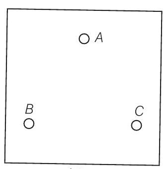
(a)
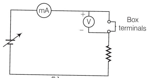
(b)
Three components namely, two germanium diodes and one resistor are connected across these three terminals in some arrangement.
A student performs an experiment in which any two of these three terminals are connected in the circuit shown in figure.
The student obtains graphs of current-voltage characteristics for unknown combination of components between the two terminals connected in the circuit. The graphs are
(i) when $A$ is positive and $B$ is negative
(c)
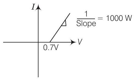
(ii) when $A$ is negative and $B$ is positive
(d)
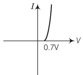
(iii) when $B$ is negative and $C$ is positive
(e) (iv) when $B$ is positive and $C$ is negative
(f)
(v) when $A$ is positive and $C$ is negative
(g)
(vi) when $A$ is negative and $C$ is positive
(h)
From these graphs of current - voltage characteristic shown in fig. (c) to (h) determine the arrangement of components between $A, B$, and $C$.
Show Answer
Answer
(a) In $V-I$ graph of condition (i), a reverse characteristics is shown in fig. (c). Here $A$ is connected to $n$ - side of $p-n$ junction $I$ and $B$ is connected to $p$-side of $p-n$ junction I with a resistance in series.
(b) In V-I graph of condition (ii), a forward characteristics is shown in fig. (d), where $0.7 V$ is the knee voltage of $p-n$ junction I $1 /$ slope $=(1 / 1000) \Omega$.
It means $A$ is connected to $n$-side of $p-n$ junction $I$ and $B$ is connected to $p$-side of $p-n$ junction $I$ and resistance $R$ is in series of $p-n$ junction $I$ between $A$ and $B$.
(c) In $V$ - $I$ graph of condition (iii), a forward characteristics is shown in figure (e), where $0.7 V$ is the knee voltage. In this case $p$-side of $p$ - $n$ junction II is connected to $C$ and $n$-side of $p$ - $n$ junction II to $B$.
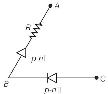
(d) In $V$ - $I$ graphs of conditions (iv), (v), (vi) also concludes the above connection of $p-n$ junctions I and II along with a resistance $R$.
Thus, the arrangement of $p-n I, p-n |$ and resistance $R$ between $A, B$ and $C$ will be as shown in the figure
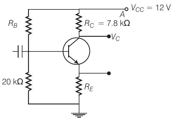
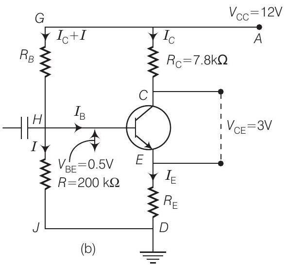
39. For the transistor circuit shown in figure, evaluate $V_{E}, R_{B}, R_{E}$, given $I_{C}=1 mA, V_{C E}=3 V, V_{B E}=0.5 V$ and $V_{C C}=12 V, \beta=100$
Show Answer
Answer
Consider the fig. (b) given here to solve this problem
$$ \begin{aligned} I_{C} & \approx I_{E} \qquad \text{[As base current is very small.]} \\ R_{C} & =7.8 k \Omega \\ \text { From the figure, } I_{C}(R_{C}+R_{E})+V_{CE} & =12 \\ (R_{E}+R_{C}) \times 1 \times 10^{-3}+3 & =12 \\ R_{E}+R_{C} & =9 \times 10^{3}=9 k \Omega \\ R_{E} & =9-7.8=1.2 k \Omega \\ V_{E} & =I_{E} \times R_{E} \\ & =1 \times 10^{-3} \times 1.2 \times 10^{3}=1.2 V \\ \text { Voltage } V_{B} & =V_{E}+V_{B E}=1.2+0.5=1.7 V \\ \text { Current } I & =\frac{V_{B}}{20 \times 10^{3}}=\frac{1.7}{20 \times 10^{3}}=0.085 mA \\ \text { Resistance } R_{B} & =\frac{12-1.7}{\frac{I_C}{\beta}+0.085}=\frac{10.3}{0.01+0.085} \qquad \text{[Given,$\beta$ =100]} \\ & =108k\Omega \end{aligned} $$
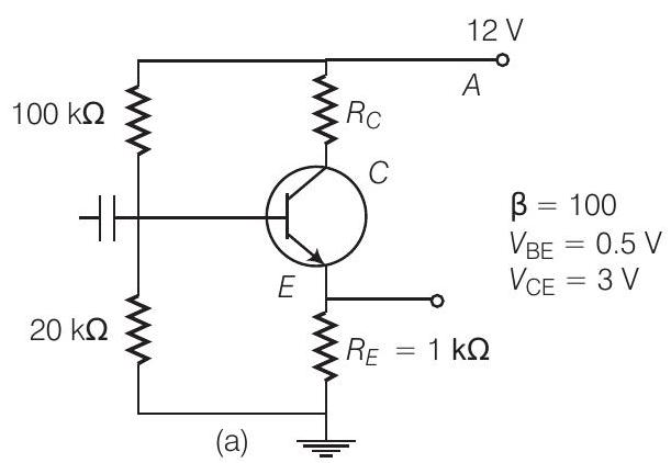
40. n the circuit shown in fig. (a), find the value of $R_{c}$.
Show Answer
Answer
Consider the fig. (b) to solve this question,
$$ \begin{aligned} I_E & =I_C+I_B \text { and } I_C=\beta I_B \qquad \text{…(i)} \\ I_C R_C+V_{C E}+I_E R_E & =V_{C C} \qquad \text{…(ii)} \\ R I_B+V_{B E}+I_E R_E & =V_{C C} \qquad \text{…(iii)} \\ \because \qquad I_E & \approx I_C=\beta I_B \end{aligned} $$
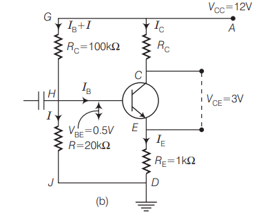
From Eq.(iii),
$$ \begin{aligned} (R+\beta R_{E}) I_{B} & =V_{CC}-V_{BE} \\ \Rightarrow \qquad I_{B} & =\frac{V_{CC}-V_{BE}}{R+\beta \cdot R_{E}} \\ & =\frac{12-0.5}{80+1.2 \times 100}=\frac{11.5}{200} mA \end{aligned} $$
From Eq.(ii),
$$ (R_{C}+R_{E})=\frac{V_{C E}-V_{B E}}{I_{C}}=\frac{V_{C C}-V_{C E}}{\beta I_{B}} \qquad(\because I_{C}=\beta I_{B}) $$
$$ \begin{aligned} (R_{C}+R_{E}) & =\frac{2}{11.5}(12-3) k \Omega=1.56 k \Omega \\ R_{C}+R_{E} & =1.56 \\ R_{C} & =1.56-1=0.56 k \Omega \end{aligned} $$